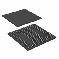
ADSP-BF538BBCZ-4F4 Analog Devices Inc, ADSP-BF538BBCZ-4F4 Datasheet - Page 48

ADSP-BF538BBCZ-4F4
Manufacturer Part Number
ADSP-BF538BBCZ-4F4
Description
IC, FLOAT-PT DSP, 16BIT, 400MHZ, BGA-316
Manufacturer
Analog Devices Inc
Series
Blackfinr
Type
Fixed Pointr
Datasheets
1.ADSP-BF538BBCZ-5F8.pdf
(56 pages)
2.ADSP-BF538BBCZ-4A.pdf
(56 pages)
3.ADSP-BF538BBCZ-4F4.pdf
(60 pages)
Specifications of ADSP-BF538BBCZ-4F4
No. Of Bits
16 Bit
Frequency
400MHz
Supply Voltage
1.2V
Embedded Interface Type
CAN, I2C, PPI, SPI, TWI, UART
No. Of I/o's
54
Flash Memory Size
512KB
Interface
CAN, SPI, SSP, TWI, UART
Clock Rate
400MHz
Non-volatile Memory
FLASH (512 kB)
On-chip Ram
148kB
Voltage - I/o
3.00V, 3.30V
Voltage - Core
1.20V
Operating Temperature
-40°C ~ 85°C
Mounting Type
Surface Mount
Package / Case
316-CSPBGA
Device Core Size
16b
Architecture
Modified Harvard
Format
Fixed Point
Clock Freq (max)
400MHz
Mips
400
Device Input Clock Speed
400MHz
Ram Size
32KB
Program Memory Size
512KB
Operating Supply Voltage (typ)
1.2/2.5/3.3V
Operating Supply Voltage (min)
0.8/2.25/2.7V
Operating Supply Voltage (max)
1.32/3.6V
Operating Temp Range
-40C to 85C
Operating Temperature Classification
Industrial
Mounting
Surface Mount
Pin Count
316
Package Type
CSPBGA
Lead Free Status / RoHS Status
Lead free / RoHS Compliant
For Use With
ADZS-BFAUDIO-EZEXT - BOARD EVAL AUDIO BLACKFIN
Lead Free Status / Rohs Status
Compliant
ADSP-BF538/ADSP-BF538F
TEST CONDITIONS
All timing parameters appearing in this data sheet were mea-
sured under the conditions described in this section.
shows the measurement point for ac measurements (except out-
put enable/disable). The measurement point V
V
OUTPUT
DDEXT
INPUT
OR
-
-
-
-
-
-
-
-
-
-
-
-
-
-
10
20
30
40
50
60
10
20
30
40
50
60
70
80
0
0
(nominal) = 3.0 V/3.3 V.
0
0
V
MEAS
Measurements (Except Output Enable/Disable)
Figure 42. Voltage Reference Levels for AC
0.5
Figure 41. Drive Current E (High V
Figure 40. Drive Current E (Low V
0.5
1.0
1.0
1.5
SOURCE VOLTAGE (V)
SOURCE VOLTAGE (V)
1.5
2.0
DDEXT
DDEXT
2.5
MEAS
2.0
)
)
V
V
V
V
V
MEAS
DDEXT
DDEXT
DDEXT
DDEXT
is 1.5 V for
Rev. D | Page 48 of 56 | July 2010
V
3.0
Figure 42
OL
= 2.75V
= 3.0 V
= 3.3 V
= 3.6 V
V
2.5
OL
3.5
3.0
4.0
Output Enable Time Measurement
Output pins are considered to be enabled when they have made
a transition from a high impedance state to the point when they
start driving.
The output enable time t
a reference signal reaches a high or low voltage level to the point
when the output starts driving as shown on the right side of
ure 43, “Output Enable/Disable,” on page
The time t
signal switches to when the output voltage reaches V
or V
V
when the output starts driving to when the output reaches the
V
Time t
If multiple pins (such as the data bus) are enabled, the measure-
ment value is that of the first pin to start driving.
Output Disable Time Measurement
Output pins are considered to be disabled when they stop driv-
ing, go into a high impedance state, and start to decay from their
output high or low voltage. The output disable time t
difference between t
side of
The time for the voltage on the bus to decay by ΔV is dependent
on the capacitive load C
time can be approximated by the equation:
The time t
ΔV equal to 0.5 V for V
The time t
signal switches, to when the output voltage decays ΔV from the
measured output high or output low voltage.
(MEASURED)
(MEASURED)
DDEXT
TRIP
t
DIS
TRIP
V
V
(high) or V
OH
OL
ENA
OUTPUT STOPS DRIVING
Figure
(nominal) = 3.0 V/3.3 V. Time t
(low). V
is calculated as shown in the equation:
ENA_MEASURED
DECAY
DIS_MEASURED
43.
t
TRIP
is calculated with test loads C
TRIP
DIS
REFERENCE
Figure 43. Output Enable/Disable
t
t
V
V
DIS_MEASURED
ENA
OH
(high) is 2.0 V and V
OL
(low) trip voltage.
SIGNAL
DIS_MEASURED
=
t
t
(MEASURED)
DECAY
(MEASURED) + V
DECAY
is the interval from when the reference
is the interval from when the reference
t
=
DDEXT
DIS_MEASURED
L
ENA
and the load current I
t
ENA_MEASURED
HIGH IMPEDANCE STATE
is the interval from the point when
=
(nominal) = 3.0 V/3.3 V.
(
t
and t
C
ENA
L
Δ
V
–
V
DECAY
t
) I
OUTPUT STARTS DRIVING
DECAY
–
TRIP
⁄
TRIP
t
L
48.
TRIP
as shown on the left
is the interval from
(low) is 1.0 V for
t
L
ENA_MEASURED
V
V
and I
TRIP
L
TRIP
t
. This decay
TRIP
(LOW)
V
V
(HIGH)
OH
OL
L
TRIP
DIS
, and with
(MEASURED)
(MEASURED)
is the
(high)
Fig-


