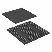
ADSP-BF538BBCZ-4F4 Analog Devices Inc, ADSP-BF538BBCZ-4F4 Datasheet - Page 23

ADSP-BF538BBCZ-4F4
Manufacturer Part Number
ADSP-BF538BBCZ-4F4
Description
IC, FLOAT-PT DSP, 16BIT, 400MHZ, BGA-316
Manufacturer
Analog Devices Inc
Series
Blackfinr
Type
Fixed Pointr
Datasheets
1.ADSP-BF538BBCZ-5F8.pdf
(56 pages)
2.ADSP-BF538BBCZ-4A.pdf
(56 pages)
3.ADSP-BF538BBCZ-4F4.pdf
(60 pages)
Specifications of ADSP-BF538BBCZ-4F4
No. Of Bits
16 Bit
Frequency
400MHz
Supply Voltage
1.2V
Embedded Interface Type
CAN, I2C, PPI, SPI, TWI, UART
No. Of I/o's
54
Flash Memory Size
512KB
Interface
CAN, SPI, SSP, TWI, UART
Clock Rate
400MHz
Non-volatile Memory
FLASH (512 kB)
On-chip Ram
148kB
Voltage - I/o
3.00V, 3.30V
Voltage - Core
1.20V
Operating Temperature
-40°C ~ 85°C
Mounting Type
Surface Mount
Package / Case
316-CSPBGA
Device Core Size
16b
Architecture
Modified Harvard
Format
Fixed Point
Clock Freq (max)
400MHz
Mips
400
Device Input Clock Speed
400MHz
Ram Size
32KB
Program Memory Size
512KB
Operating Supply Voltage (typ)
1.2/2.5/3.3V
Operating Supply Voltage (min)
0.8/2.25/2.7V
Operating Supply Voltage (max)
1.32/3.6V
Operating Temp Range
-40C to 85C
Operating Temperature Classification
Industrial
Mounting
Surface Mount
Pin Count
316
Package Type
CSPBGA
Lead Free Status / RoHS Status
Lead free / RoHS Compliant
For Use With
ADZS-BFAUDIO-EZEXT - BOARD EVAL AUDIO BLACKFIN
Lead Free Status / Rohs Status
Compliant
SPECIFICATIONS
Note that component specifications are subject to change
without notice.
OPERATING CONDITIONS
1
2
3
4
5
6
Parameter
V
V
V
V
V
V
V
V
V
V
T
The regulator can generate V
See
The 3.3 V tolerant pins are capable of accepting up to 3.6 V maximum V
The 5 V tolerant pins are capable of accepting up to 5.5 V maximum V
Parameter value applies to the CLKIN input pin.
Parameter value applies to all input and bidirectional pins.
PF15–0, PPI3–0, SPI1SS, SPI1SEL1, PC9–5, SPI2SS, SPI2SEL1, RX2–1, TX2–1, TSCLK3–0, RSCLK3–0, TFS3–0, RFS3–0, DT2PRI, DT2SEC, DR2PRI, DR2SEC, DT3PRI,
DT3SEC, DR3PRI, DR3SEC, and TMR2–0. The following input-only pins are 3.3 V tolerant: RESET, RX0, TCK, TDI, TMS, TRST, ARDY, BMODE1–0, BR, DR0PRI,
DR0SEC, DR1PRI, DR1SEC, NMI, PPI_CLK, and RTXI.
PC4. The following input-only pin is 5 V tolerant: GPW.
DDINT
DDINT
DDEXT
DDEXT
DDRTC
IH
IH5V
IHCLKIN
IL
IL5V
J
Ordering Guide on Page
Internal Supply Voltage
Internal Supply Voltage
External Supply Voltage
External Supply Voltage
Real-Time Clock Power Supply
Voltage
High Level Input Voltage
High Level Input Voltage
High Level Input Voltage
Low Level Input Voltage
Low Level Input Voltage
Junction Temperature
56.
DDINT
at levels of 0.85 V to 1.2 V with –5% to +10% tolerance and 1.25 V with –4% to +10% tolerance
3, 6
4
3
4
5
533 MHz Speed Grade Models
400 MHz Speed Grade Models
Models with on-chip flash
V
V
V
V
V
316-Ball Chip Scale Package Ball Grid Array (CSP_BGA)
@ T
Conditions
Models without on-chip flash
DDEXT
DDEXT
DDEXT
DDEXT
DDEXT
AMBIENT
= Minimum
= Maximum
= Maximum
= Maximum
= Minimum
= –40°C to +85°C
Rev. D | Page 23 of 56 | July 2010
IH
. The following bidirectional pins are 5 V tolerant: SCL0, SCL1, SDA0, SDA1, CANTX, CANRX, and
IH
The following bidirectional pins are 3.3 V tolerant: DATA15–0, SCK2–0, MISO2–0, MOSI2–0,
2
2
1, 2
1, 2
ADSP-BF538/ADSP-BF538F
Min
0.8
0.8
2.7
2.25
2.25
2.0
2.0
2.2
–40
Nom
1.25
1.2
3.3
3.0
Max
1.375
1.32
3.6
3.6
3.6
+0.6
+0.8
+110
Unit
V
V
V
V
V
V
V
V
V
V
°C


