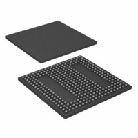
ADSP-BF538BBCZ-4F4 Analog Devices Inc, ADSP-BF538BBCZ-4F4 Datasheet - Page 15

ADSP-BF538BBCZ-4F4
Manufacturer Part Number
ADSP-BF538BBCZ-4F4
Description
IC, FLOAT-PT DSP, 16BIT, 400MHZ, BGA-316
Manufacturer
Analog Devices Inc
Series
Blackfinr
Type
Fixed Pointr
Datasheets
1.ADSP-BF538BBCZ-5F8.pdf
(56 pages)
2.ADSP-BF538BBCZ-4A.pdf
(56 pages)
3.ADSP-BF538BBCZ-4F4.pdf
(60 pages)
Specifications of ADSP-BF538BBCZ-4F4
No. Of Bits
16 Bit
Frequency
400MHz
Supply Voltage
1.2V
Embedded Interface Type
CAN, I2C, PPI, SPI, TWI, UART
No. Of I/o's
54
Flash Memory Size
512KB
Interface
CAN, SPI, SSP, TWI, UART
Clock Rate
400MHz
Non-volatile Memory
FLASH (512 kB)
On-chip Ram
148kB
Voltage - I/o
3.00V, 3.30V
Voltage - Core
1.20V
Operating Temperature
-40°C ~ 85°C
Mounting Type
Surface Mount
Package / Case
316-CSPBGA
Device Core Size
16b
Architecture
Modified Harvard
Format
Fixed Point
Clock Freq (max)
400MHz
Mips
400
Device Input Clock Speed
400MHz
Ram Size
32KB
Program Memory Size
512KB
Operating Supply Voltage (typ)
1.2/2.5/3.3V
Operating Supply Voltage (min)
0.8/2.25/2.7V
Operating Supply Voltage (max)
1.32/3.6V
Operating Temp Range
-40C to 85C
Operating Temperature Classification
Industrial
Mounting
Surface Mount
Pin Count
316
Package Type
CSPBGA
Lead Free Status / RoHS Status
Lead free / RoHS Compliant
For Use With
ADZS-BFAUDIO-EZEXT - BOARD EVAL AUDIO BLACKFIN
Lead Free Status / Rohs Status
Compliant
If an external clock is used, it should be a TTL-compatible signal
and must not be halted, changed, or operated below the speci-
fied frequency during normal operation. This signal is
connected to the processor’s CLKIN pin. When an external
clock is used, the XTAL pin must be left unconnected.
Alternatively, because the ADSP-BF538/ADSP-BF538F proces-
sors include an on-chip oscillator circuit, an external crystal
may be used. For fundamental frequency operation, use the cir-
cuit shown in
frequency, microprocessor-grade crystal is connected across the
CLKIN and XTAL pins. The on-chip resistance between CLKIN
and the XTAL pin is in the 500 kW range. Further parallel resis-
tors are typically not recommended. The two capacitors and the
series resistor, shown in
tude of the sine frequency. The capacitor and resistor values,
shown in
are dependent upon the crystal manufacturer's load capacitance
recommendations and the physical PCB layout. The resistor
value depends on the drive level specified by the crystal manu-
facturer. System designs should verify the customized values
based on careful investigation on multiple devices over the
allowed temperature range.
A third-overtone crystal can be used at frequencies above
25 MHz. The circuit is then modified to ensure crystal operation
only at the third overtone, by adding a tuned inductor circuit as
shown in
As shown in
peripheral clock (SCLK) are derived from the input clock
(CLKIN) signal. An on-chip PLL is capable of multiplying the
CLKIN signal by a user programmable 0.5× to 64× multiplica-
tion factor (bounded by specified minimum and maximum
VCO frequencies). The default multiplier is 10×, but it can be
modified by a software instruction sequence. On-the-fly fre-
quency changes can be effected by simply writing to the
PLL_DIV register.
CLKOUT
NOTE: VALUES MARKED WITH * MUST BE CUSTOMIZED
DEPENDING ON THE CRYSTAL AND LAYOUT. PLEASE
ANALYZE CAREFULLY.
Figure
Figure
Figure
CLKIN
Figure
EN
Figure 7. External Crystal Connections
7, are typical values only. The capacitor values
7.
8, the core clock (CCLK) and system
7. A parallel-resonant, fundamental
18pF*
Blackfin
Figure
TO PLL CIRCUITRY
XTAL
7, fine tune the phase and ampli-
0: *
18pF*
700:
FOR OVERTONE
OPERATION ONLY
V
DDEXT
1M:
Rev. D | Page 15 of 56 | July 2010
All on-chip peripherals are clocked by the system clock (SCLK).
The system clock frequency is programmable by means of the
SSEL3–0 bits of the PLL_DIV register. The values programmed
into the SSEL fields define a divide ratio between the PLL output
(VCO) and the system clock. SCLK divider values are 1
through 15.
Table 7
Table 7. Example System Clock Ratios
The maximum frequency of the system clock is f
the divisor ratio must be chosen to limit the system clock fre-
quency to its maximum of f
dynamically without any PLL lock latencies by writing the
appropriate values to the PLL divisor register (PLL_DIV).
Note that when the SSEL value is changed, it will affect all the
peripherals that derive their clock signals from the SCLK signal.
The core clock (CCLK) frequency can also be dynamically
changed by means of the CSEL1–0 bits of the PLL_DIV register.
Supported CCLK divider ratios are 1, 2, 4, and 8, as shown in
Table
fast core frequency modifications.
Table 8. Core Clock Ratios
Signal Name
SSEL3–0
0001
0110
1010
Signal Name
CSEL1–0
00
01
10
11
CLKIN
8. This programmable core clock capability is useful for
illustrates typical system clock ratios:
REQUIRES PLL SEQUENCING
“FINE” ADJUSTMENT
Figure 8. Frequency Modification Methods
0.5uTO 64u
Divider Ratio
VCO/SCLK
1:1
6:1
10:1
Divider Ratio
VCO/CCLK
1:1
2:1
4:1
8:1
PLL
ADSP-BF538/ADSP-BF538F
SCLK
Example Frequency Ratios (MHz)
VCO
100
300
500
. The SSEL value can be changed
VCO
Example Frequency Ratios
VCO
300
300
500
200
SCLK d 133MHz
SCLK d CCLK
“COARSE” ADJUSTMENT
÷ 1, 2, 4, 8
÷ 1:15
ON-THE-FLY
SCLK
100
50
50
CCLK
300
150
125
25
SCLK
. Note that
CCLK
SCLK


