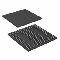
ADSP-BF538BBCZ-4F4 Analog Devices Inc, ADSP-BF538BBCZ-4F4 Datasheet - Page 28

ADSP-BF538BBCZ-4F4
Manufacturer Part Number
ADSP-BF538BBCZ-4F4
Description
IC, FLOAT-PT DSP, 16BIT, 400MHZ, BGA-316
Manufacturer
Analog Devices Inc
Series
Blackfinr
Type
Fixed Pointr
Datasheets
1.ADSP-BF538BBCZ-5F8.pdf
(56 pages)
2.ADSP-BF538BBCZ-4A.pdf
(56 pages)
3.ADSP-BF538BBCZ-4F4.pdf
(60 pages)
Specifications of ADSP-BF538BBCZ-4F4
No. Of Bits
16 Bit
Frequency
400MHz
Supply Voltage
1.2V
Embedded Interface Type
CAN, I2C, PPI, SPI, TWI, UART
No. Of I/o's
54
Flash Memory Size
512KB
Interface
CAN, SPI, SSP, TWI, UART
Clock Rate
400MHz
Non-volatile Memory
FLASH (512 kB)
On-chip Ram
148kB
Voltage - I/o
3.00V, 3.30V
Voltage - Core
1.20V
Operating Temperature
-40°C ~ 85°C
Mounting Type
Surface Mount
Package / Case
316-CSPBGA
Device Core Size
16b
Architecture
Modified Harvard
Format
Fixed Point
Clock Freq (max)
400MHz
Mips
400
Device Input Clock Speed
400MHz
Ram Size
32KB
Program Memory Size
512KB
Operating Supply Voltage (typ)
1.2/2.5/3.3V
Operating Supply Voltage (min)
0.8/2.25/2.7V
Operating Supply Voltage (max)
1.32/3.6V
Operating Temp Range
-40C to 85C
Operating Temperature Classification
Industrial
Mounting
Surface Mount
Pin Count
316
Package Type
CSPBGA
Lead Free Status / RoHS Status
Lead free / RoHS Compliant
For Use With
ADZS-BFAUDIO-EZEXT - BOARD EVAL AUDIO BLACKFIN
Lead Free Status / Rohs Status
Compliant
ADSP-BF538/ADSP-BF538F
TIMING SPECIFICATIONS
Component specifications are subject to change
with PCN notice.
Clock and Reset Timing
Table 21
Absolute Maximum Ratings on Page
CLKIN and clock multipliers must not select core/peripheral
clocks that exceed maximum operating conditions.
Table 21. Clock and Reset Timing
1
2
3
4
5
6
Table 22. Power-Up Reset Timing
Parameter
Timing Requirements
t
Parameter
Timing Requirements
f
t
t
t
t
Applies to PLL bypass mode and PLL nonbypass mode.
Combinations of the CLKIN frequency and the PLL clock multiplier must not exceed the allowed f
The t
If the DF bit in the PLL_CTL register is set, the minimum f
Applies after power-up sequence is complete. See
Applies when processor is configured in No Boot Mode (BMODE2-0 = b#000).
RST_IN_PWR
CKIN
CKINL
CKINH
WRST
NOBOOT
Table 16 on Page
CKIN
period (see
and
V
DD_SUPPLIES
RESET
CLKIN
Figure 10
RESET Deasserted after the V
Specification
26.
Figure
CLKIN Frequency (Commercial/ Industrial Models)
CLKIN Low Pulse
CLKIN High Pulse
RESET Asserted Pulse Width Low
RESET Deassertion to First External Access Delay
RESET
CLKIN
10) equals 1/f
describe clock and reset operations. Per
CKIN
t
CKINL
1
1
.
27, combinations of
t
CKIN
Table 22
DDINT
t
CKINH
, V
In
CKIN
and
DDEXT
Figure
specification is 24 MHz for commercial/industrial models.
Figure 11
5
Rev. D | Page 28 of 56 | July 2010
, V
t
RST_IN_PWR
Figure 10. Clock and Reset Timing
Figure 11. Power-Up Reset Timing
DDRTC
11, V
t
WRST
for power-up reset timing.
, and CLKIN Pins are Stable and Within
DD_SUPPLIES
6
1, 2, 3, 4
is V
DDINT
Min
10
8
8
11 × t
3 × t
, V
CKIN
VCO
DDEXT
CKIN
, f
CCLK
, V
t
NOBOOT
DDRTC
, and f
SCLK
settings discussed in
Max
50
5 × t
Min
3500 × t
CKIN
Table 11 on Page 24
CKIN
Max
through
Unit
ns
MHz
Unit
ns
ns
ns
ns


