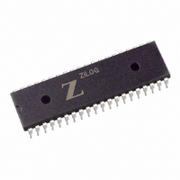
Z85C3010PSG Zilog, Z85C3010PSG Datasheet - Page 108

Z85C3010PSG
Manufacturer Part Number
Z85C3010PSG
Description
IC 10MHZ Z8500 CMOS SCC 40-DIP
Manufacturer
Zilog
Series
SCCr
Specifications of Z85C3010PSG
Processor Type
Z80
Features
Error Detection and Multiprotocol Support
Speed
10MHz
Voltage
5V
Mounting Type
Through Hole
Package / Case
40-DIP (0.620", 15.75mm)
Cpu Speed
8MHz
Digital Ic Case Style
DIP
No. Of Pins
40
Supply Voltage Range
5V
Operating Temperature Range
0°C To +70°C
Svhc
No SVHC (18-Jun-2010)
Base Number
85
Rohs Compliant
Yes
Clock Frequency
10MHz
Lead Free Status / RoHS Status
Lead free / RoHS Compliant
Other names
269-3934
Z85C3010PSG
Z85C3010PSG
Available stocks
Company
Part Number
Manufacturer
Quantity
Price
Company:
Part Number:
Z85C3010PSG
Manufacturer:
Zilog
Quantity:
135
Company:
Part Number:
Z85C3010PSG
Manufacturer:
Zilog
Quantity:
326
- Current page: 108 of 317
- Download datasheet (4Mb)
UM010901-0601
5.1 INTRODUCTION
This section describes the functions of the various bits in
the registers of the SCC (Tables 5-1 and 5-2). Reserved
bits are not used in this implementation of the device and
may or may not be physically present in the device. For the
register addresses, also refer to Tables 2-1, 2-2 and 2-5 in
Chapter 2. Reserved bits that are physically present are
.
Notes for Tables 5-1 and 5-2:
Reg
WR0
WR1
WR2
WR3
WR4
WR5
WR6
WR7
WR7'
WR8
WR9
WR10
WR11 Clock mode controls for receive and transmit
WR12 Lower byte of baud rate generator
WR13 Upper byte of baud rate generator
WR14 Miscellaneous control bits
WR15 External status interrupt enable control
1. ESCC and 85C30 only.
2. On the ESCC and 85C30, these registers are readable as
3. This feature is not available on NMOS.
RR9, RR4, RR5, and RR11, respectively, when WR7' D6=1.
Refer to the description of WR7 Prime for enabling the ex-
tended read capability.
2
2
2
1
2
Description
Reg. pointers, various initialization commands
Transmit and Receive interrupt enables,
WAIT/DMA commands
Interrupt Vector
Receive parameters and control modes
Transmit and Receive modes and parameters
Transmit parameters and control modes
Sync Character or SDLC address
Sync Character or SDLC flag
Extended Feature and FIFO Control
(WR7 Prime)
Transmit buffer
Master Interrupt control and reset commands
Miscellaneous transmit and receive control bits
Table 5-1. SCC Write Registers
U
C
R
readable and writable but reserved bits that are not present
will always be read as zero. To ensure compatibility with fu-
ture versions of the device, reserved bits should always be
written with zeros. Reserved commands are not used for
the same reason.
Reg
RR0
RR1
RR2
RR3
RR4
RR5
RR6
RR7
RR8
RR9
RR10
RR11
RR12
RR13
RR14
RR15
SER
EGISTER
HAPTER
2
2
3
3
2
2
2
’
S
Description
Transmit and Receive buffer status and external
status
Special Receive Condition status
Modified interrupt vector (Channel B only),
Unmodified interrupt vector (Channel A only)
Interrupt pending bits (Channel A only)
Transmit and Receive modes and parameters
(WR4)
Transmit parameters and control modes (WR5)
SDLC FIFO byte counter lower byte (only when
enabled)
SDLC FIFO byte count and status (only when
enabled)
Receive buffer
Receive parameters and control modes (WR3)
Miscellaneous status bits
Miscellaneous transmit and receive control bits
(WR10)
Lower byte of baud rate generator time constant
Upper byte of baud rate generator time constant
Extended Feature and FIFO Control (WR7
Prime)
External Status interrupt information
M
Table 5-2. SCC Read Registers
ANUAL
D
ESCRIPTIONS
5
5-1
5
Related parts for Z85C3010PSG
Image
Part Number
Description
Manufacturer
Datasheet
Request
R

Part Number:
Description:
Manufacturer:
Zilog, Inc.
Datasheet:

Part Number:
Description:
Cmos Scc Serial Communications Controller
Manufacturer:
ZiLOG Semiconductor
Datasheet:

Part Number:
Description:
Communication Controllers, ZILOG INTELLIGENT PERIPHERAL CONTROLLER (ZIP)
Manufacturer:
Zilog, Inc.
Datasheet:

Part Number:
Description:
KIT DEV FOR Z8 ENCORE 16K TO 64K
Manufacturer:
Zilog
Datasheet:

Part Number:
Description:
KIT DEV Z8 ENCORE XP 28-PIN
Manufacturer:
Zilog
Datasheet:

Part Number:
Description:
DEV KIT FOR Z8 ENCORE 8K/4K
Manufacturer:
Zilog
Datasheet:

Part Number:
Description:
KIT DEV Z8 ENCORE XP 28-PIN
Manufacturer:
Zilog
Datasheet:

Part Number:
Description:
DEV KIT FOR Z8 ENCORE 4K TO 8K
Manufacturer:
Zilog
Datasheet:

Part Number:
Description:
CMOS Z8 microcontroller. ROM 16 Kbytes, RAM 256 bytes, speed 16 MHz, 32 lines I/O, 3.0V to 5.5V
Manufacturer:
Zilog, Inc.
Datasheet:

Part Number:
Description:
Low-cost microcontroller. 512 bytes ROM, 61 bytes RAM, 8 MHz
Manufacturer:
Zilog, Inc.
Datasheet:

Part Number:
Description:
Z8 4K OTP Microcontroller
Manufacturer:
Zilog, Inc.
Datasheet:

Part Number:
Description:
CMOS SUPER8 ROMLESS MCU
Manufacturer:
Zilog, Inc.
Datasheet:

Part Number:
Description:
SL1866 CMOSZ8 OTP Microcontroller
Manufacturer:
Zilog, Inc.
Datasheet:


