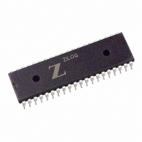
Z85C3010PSG Zilog, Z85C3010PSG Datasheet - Page 133

Z85C3010PSG
Manufacturer Part Number
Z85C3010PSG
Description
IC 10MHZ Z8500 CMOS SCC 40-DIP
Manufacturer
Zilog
Series
SCCr
Specifications of Z85C3010PSG
Processor Type
Z80
Features
Error Detection and Multiprotocol Support
Speed
10MHz
Voltage
5V
Mounting Type
Through Hole
Package / Case
40-DIP (0.620", 15.75mm)
Cpu Speed
8MHz
Digital Ic Case Style
DIP
No. Of Pins
40
Supply Voltage Range
5V
Operating Temperature Range
0°C To +70°C
Svhc
No SVHC (18-Jun-2010)
Base Number
85
Rohs Compliant
Yes
Clock Frequency
10MHz
Lead Free Status / RoHS Status
Lead free / RoHS Compliant
Other names
269-3934
Z85C3010PSG
Z85C3010PSG
Available stocks
Company
Part Number
Manufacturer
Quantity
Price
Company:
Part Number:
Z85C3010PSG
Manufacturer:
Zilog
Quantity:
135
Company:
Part Number:
Z85C3010PSG
Manufacturer:
Zilog
Quantity:
326
- Current page: 133 of 317
- Download datasheet (4Mb)
SCC™/ESCC™ User’s Manual
Register Descriptions
5.3 READ REGISTERS (Continued)
If the FIFO overflows, the FIFO and the FIFO Overflow
Status bit are cleared by disabling and then re-enabling the
FIFO through the FIFO control bit (WR15, D2). Otherwise,
this register returns an image of RR3.
On the NMOS version, a read to this location returns an
image of RR3.
5.3.9 Read Register 8
RR8 is the Receive Data register.
5.3.10 Read Register 9 (ESCC and 85C30
Only)
On the ESCC, Read Register 9 reflects the contents of
Write Register 3 provided the Extended Read option has
been enabled.
On the NMOS/CMOS version, a read to this location re-
turns an image of RR13.
5-26
Table 5-13. .Read Register 7 FIFO Status Decoding
Bit D7
Bit D6
Read Register 7
D7 D6 D5 D4 D3 D2 D1 D0
*
1
0
1
0
Can only be accessed if the SDLC FIFO enhancement
SDLC FIFO Status and Byte Count (MSB)
Figure 5-24. Read Register 7 (Not on NMOS)
is enabled (WR15 bit D2 set to 1)
*
FIFO Data Available Status
Status reads come from FIFO
(FIFO is not Empty)
Status reads bypass FIFO
because FIFO is Empty)
FIFO Overflow Status
FIFO has overflowed
Normal operation
BC8
BC9
BC10
BC11
BC12
BC13
FDA: FIFO Data Available
1 = Status Reads from FIFO
0 = Status Reads from ESCC
FOS: FIFO Overflow Status
1 = FIFO Overflowed
0 = Normal
5.3.11 Read Register 10
RR10 contains some miscellaneous status bits. Unused
bits are always 0. Bit positions for RR10 are shown in
Figure 5-25.
Bit 7: One Clock Missing status
While operating in the FM mode, the DPLL sets this bit to
1 when it does not see a clock edge on the incoming lines
in the window where it expects one. This bit is latched until
reset by a Reset Missing Clock or Enter Search Mode
command in WR14. In the NRZI mode of operation and
while the DPLL is disabled, this bit is always 0.
Bit 6: Two Clocks Missing status
While operating in the FM mode, the DPLL sets this bit to
1 when it does not see a clock edge in two successive
tries. At the same time the DPLL enters the Search mode.
This bit is latched until reset by a Reset Missing Clock or
Enter Search Mode command in WR14, bit 5-7. In the
NRZI mode of operation and while the DPLL is disabled,
this bit is always 0.
Bit 4: Loop Sending status
This bit is set to 1 in SDLC Loop mode while the transmitter
is in control of the Loop, that is, while the SCC is actively
transmitting on the loop. This bit is reset at all other times.
This bit can be polled in SDLC mode to determine when
the closing flag has been sent.
Bit 1: On Loop status
This bit is set to 1 while the SCC is actually on loop in
SDLC Loop mode. This bit is set to 1 in the X21 mode
(Loop mode selected while in monosync) when the trans-
mitter goes active. This bit is 0 at all other times. This bit
can also be pulled in SDLC mode to determine when the
closing flag has been sent.
Read Register 10
D7 D6 D5 D4 D3
Figure 5-25. Read Register 10
D2 D1 D0
0
On Loop
0
0
Loop Sending
0
Two Clocks Missing
One Clock Missing
UM010901-0601
Related parts for Z85C3010PSG
Image
Part Number
Description
Manufacturer
Datasheet
Request
R

Part Number:
Description:
Manufacturer:
Zilog, Inc.
Datasheet:

Part Number:
Description:
Cmos Scc Serial Communications Controller
Manufacturer:
ZiLOG Semiconductor
Datasheet:

Part Number:
Description:
Communication Controllers, ZILOG INTELLIGENT PERIPHERAL CONTROLLER (ZIP)
Manufacturer:
Zilog, Inc.
Datasheet:

Part Number:
Description:
KIT DEV FOR Z8 ENCORE 16K TO 64K
Manufacturer:
Zilog
Datasheet:

Part Number:
Description:
KIT DEV Z8 ENCORE XP 28-PIN
Manufacturer:
Zilog
Datasheet:

Part Number:
Description:
DEV KIT FOR Z8 ENCORE 8K/4K
Manufacturer:
Zilog
Datasheet:

Part Number:
Description:
KIT DEV Z8 ENCORE XP 28-PIN
Manufacturer:
Zilog
Datasheet:

Part Number:
Description:
DEV KIT FOR Z8 ENCORE 4K TO 8K
Manufacturer:
Zilog
Datasheet:

Part Number:
Description:
CMOS Z8 microcontroller. ROM 16 Kbytes, RAM 256 bytes, speed 16 MHz, 32 lines I/O, 3.0V to 5.5V
Manufacturer:
Zilog, Inc.
Datasheet:

Part Number:
Description:
Low-cost microcontroller. 512 bytes ROM, 61 bytes RAM, 8 MHz
Manufacturer:
Zilog, Inc.
Datasheet:

Part Number:
Description:
Z8 4K OTP Microcontroller
Manufacturer:
Zilog, Inc.
Datasheet:

Part Number:
Description:
CMOS SUPER8 ROMLESS MCU
Manufacturer:
Zilog, Inc.
Datasheet:

Part Number:
Description:
SL1866 CMOSZ8 OTP Microcontroller
Manufacturer:
Zilog, Inc.
Datasheet:


