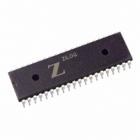
Z85C3010PSG Zilog, Z85C3010PSG Datasheet - Page 131

Z85C3010PSG
Manufacturer Part Number
Z85C3010PSG
Description
IC 10MHZ Z8500 CMOS SCC 40-DIP
Manufacturer
Zilog
Series
SCCr
Specifications of Z85C3010PSG
Processor Type
Z80
Features
Error Detection and Multiprotocol Support
Speed
10MHz
Voltage
5V
Mounting Type
Through Hole
Package / Case
40-DIP (0.620", 15.75mm)
Cpu Speed
8MHz
Digital Ic Case Style
DIP
No. Of Pins
40
Supply Voltage Range
5V
Operating Temperature Range
0°C To +70°C
Svhc
No SVHC (18-Jun-2010)
Base Number
85
Rohs Compliant
Yes
Clock Frequency
10MHz
Lead Free Status / RoHS Status
Lead free / RoHS Compliant
Other names
269-3934
Z85C3010PSG
Z85C3010PSG
Available stocks
Company
Part Number
Manufacturer
Quantity
Price
Company:
Part Number:
Z85C3010PSG
Manufacturer:
Zilog
Quantity:
135
Company:
Part Number:
Z85C3010PSG
Manufacturer:
Zilog
Quantity:
326
- Current page: 131 of 317
- Download datasheet (4Mb)
SCC™/ESCC™ User’s Manual
Register Descriptions
5.3 READ REGISTERS (Continued)
Also, a Special Receive Condition vector is returned,
caused by the overrun characters and all subsequent char-
acters received until the Error Reset command is issued.
On the CMOS and ESCC, if the Status FIFO is enabled
(refer to the description in Write Register 15, bit D2 and the
description in Read Register 7, bits D7 and D6), this bit re-
flects the status stored at the exit location of the Status
FIFO.
Bit 4: Parity Error status.
When parity is enabled, this bit is set for the characters
whose parity does not match the programmed sense
(even/odd). This bit is latched so that once an error occurs,
it remains set until the Error Reset command is issued. If
the parity in Special Condition bit is set, a parity error caus-
es a Special Receive Condition vector to be returned on
the character containing the error and on all subsequent
characters until the Error Reset command is issued.
Bits 3, 2, and 1: Residue Codes, bits 2, 1, and 0
In those cases in SDLC mode where the received I-Field
Bit 0: All Sent status
In Asynchronous mode, this bit is set when all characters
have completely cleared the transmitter pins. Most mo-
dems contain additional delays in the data path, which re-
quires the modem control signals to remain active until af-
ter the data has cleared both the transmitter and the
modem. This bit is always set in synchronous and SDLC
modes.
5-24
Table 5-12. Bits per Character Residue Decoding
Bits per Character
Bit 3
8
7
6
5
1
0
1
0
1
0
1
0
Bit 3
0
0
0
0
Bit 2
Table 5-11. I-Field Bit Selection (8 Bits Only)
0
1
1
0
0
1
1
0
Bit 2
1
0
1
0
Bit 1
1
0
0
1
Bit 1
0
0
0
1
1
1
1
0
is not an integral multiple of the character length, these
three bits indicate the length of the I-Field and are mean-
ingful only for the transfer in which the end of frame bit is
set. This field is set to 011 by a channel or hardware reset
and is forced to this state in Asynchronous mode. These
three bits can leave this state only if SDLC is selected and
a character is received. The codes signify the following
(Reference Table 5-11) when a receive character length is
eight bits per character.
On the CMOS and ESCC, if the Status FIFO is enabled
(refer to the description in Write Register 15, bit D2 and the
description in Read Register 7, bits D7 and D6), these bits
reflect the status stored at the exit location of the Status
FIFO.
I-Field bits are right-justified in all cases. If a receive
character length other than eight bits is used for the I-Field,
a table similar to Table 5-11 can be constructed for each
different character length. Table 5-12 shows the residue
codes for no residue (The I-Field boundary lies on a
character boundary).
5.3.3 Read Register 2
RR2 contains the interrupt vector written into WR2. When
the register is accessed in Channel A, the vector returned
is the vector actually stored in WR2. When this register is
accessed in Channel B, the vector returned includes
status information in bits 1, 2 and 3 or in bits 6, 5 and 4,
depending on the state of the Status High/Status Low bit
in WR9 and independent of the state of the VIS bit in
WR9. The vector is modified according to Table 5-6
shown in the explanation of the VIS bit in WR9 (Section
5.2.11). If no interrupts are pending, the status is
V3,V2,V1 -011, or V6,V5,V4-110. Figure 5-21 shows the
bit positions for RR2.
I-Field Bits in Last
Byte
0
0
0
0
0
0
1
2
Previous Byte
I-Field Bits in
UM010901-0601
3
4
5
6
7
8
8
8
Related parts for Z85C3010PSG
Image
Part Number
Description
Manufacturer
Datasheet
Request
R

Part Number:
Description:
Manufacturer:
Zilog, Inc.
Datasheet:

Part Number:
Description:
Cmos Scc Serial Communications Controller
Manufacturer:
ZiLOG Semiconductor
Datasheet:

Part Number:
Description:
Communication Controllers, ZILOG INTELLIGENT PERIPHERAL CONTROLLER (ZIP)
Manufacturer:
Zilog, Inc.
Datasheet:

Part Number:
Description:
KIT DEV FOR Z8 ENCORE 16K TO 64K
Manufacturer:
Zilog
Datasheet:

Part Number:
Description:
KIT DEV Z8 ENCORE XP 28-PIN
Manufacturer:
Zilog
Datasheet:

Part Number:
Description:
DEV KIT FOR Z8 ENCORE 8K/4K
Manufacturer:
Zilog
Datasheet:

Part Number:
Description:
KIT DEV Z8 ENCORE XP 28-PIN
Manufacturer:
Zilog
Datasheet:

Part Number:
Description:
DEV KIT FOR Z8 ENCORE 4K TO 8K
Manufacturer:
Zilog
Datasheet:

Part Number:
Description:
CMOS Z8 microcontroller. ROM 16 Kbytes, RAM 256 bytes, speed 16 MHz, 32 lines I/O, 3.0V to 5.5V
Manufacturer:
Zilog, Inc.
Datasheet:

Part Number:
Description:
Low-cost microcontroller. 512 bytes ROM, 61 bytes RAM, 8 MHz
Manufacturer:
Zilog, Inc.
Datasheet:

Part Number:
Description:
Z8 4K OTP Microcontroller
Manufacturer:
Zilog, Inc.
Datasheet:

Part Number:
Description:
CMOS SUPER8 ROMLESS MCU
Manufacturer:
Zilog, Inc.
Datasheet:

Part Number:
Description:
SL1866 CMOSZ8 OTP Microcontroller
Manufacturer:
Zilog, Inc.
Datasheet:


