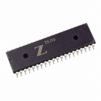
Z85C3010PSG Zilog, Z85C3010PSG Datasheet - Page 181

Z85C3010PSG
Manufacturer Part Number
Z85C3010PSG
Description
IC 10MHZ Z8500 CMOS SCC 40-DIP
Manufacturer
Zilog
Series
SCCr
Specifications of Z85C3010PSG
Processor Type
Z80
Features
Error Detection and Multiprotocol Support
Speed
10MHz
Voltage
5V
Mounting Type
Through Hole
Package / Case
40-DIP (0.620", 15.75mm)
Cpu Speed
8MHz
Digital Ic Case Style
DIP
No. Of Pins
40
Supply Voltage Range
5V
Operating Temperature Range
0°C To +70°C
Svhc
No SVHC (18-Jun-2010)
Base Number
85
Rohs Compliant
Yes
Clock Frequency
10MHz
Lead Free Status / RoHS Status
Lead free / RoHS Compliant
Other names
269-3934
Z85C3010PSG
Z85C3010PSG
Available stocks
Company
Part Number
Manufacturer
Quantity
Price
Company:
Part Number:
Z85C3010PSG
Manufacturer:
Zilog
Quantity:
135
Company:
Part Number:
Z85C3010PSG
Manufacturer:
Zilog
Quantity:
326
- Current page: 181 of 317
- Download datasheet (4Mb)
Application Note
The Z180™ Interfaced with the SCC at MHZ
System Checkout
After completion of the board (PC board or wire wrapped
board, etc.), the following methods verify that the board is
working.
Software Considerations
Based on the previous discussion, it is necessary to
program the Z180 internal registers, as follows, before
system checkout:
SCC Read Cycle Proof
Read cycle checking is first because it is the simplest
operation. The SCC Read cycle is checked by reading the
bits in RR0. First, the SCC is hardware reset by
simultaneously pulling /RD and /WR LOW (The circuit
above includes the circuit for this). Then, reading out the
Read Register 0 returns:
SCC Write Cycle Proof
Write cycle checking involves writing to a register and
reading back the results to the registers which return the
written value. The Time Constant registers (WR12 and
WR13) and External/Status Interrupt Enable register
(WR15) are on the SCC.
6-46
(Continued)
Z80 mode of operation - Clear /M1E bit in OMCR
register to zero (to provide expansion for Z80
peripherals).
Z80 compatible mode - Clear IOC bit in OMCR register
to zero.
Put one wait state in memory cycle, and no wait state for
I/O cycle DMCR register bits 7 and 6 to “1” and bits 5 and
4 to “0”.
D7-D0 = 01xxx100b
Bit D2, D6:1
Bit D7, D1, D0:0
Bit D5: Reflects /CTS pin
Bit D4: Reflects /SYNC
Bit D3: Reflects /DCD pin
Interrupt Acknowledge Cycle
Checking an Interrupt Acknowledge (/INTACK) cycle
consists of several steps. First, the SCC makes an
Interrupt Request (/INT) to the Z180. When the processor
is ready to service the interrupt, it shows an Interrupt
Acknowledge (/INTACK) cycle. The SCC then puts an 8-
bit vector on the bus and the Z180 uses that vector to get
the correct service routine. The following test checks the
simplest case.
First, load the Interrupt Vector Register (WR2) with a
vector, disable the Vector Interrupt Status (VIS) and
enable interrupts (IE=1, MIE=1 IEI=1). Disabling VIS
guarantees only one vector on the bus. The address of the
service routine corresponding to the 8-bit vector number
loads the Z180 vector table, and the Z180 is under
Interrupt Mode 2.
Because the user cannot set the SCC Interrupt Pending Bit
(IP), setting an interrupt sequence is difficult. An interrupt
is generated indirectly via the CTS pin by enabling the
following explanation.
Enable interrupt by /CTS (WR15, 20h), External/Status
Interrupt Enable (WR1, 01h), and Master Interrupt Enable
(WR9, 08h). Any change on the /CTS pin begins the
interrupt sequence. The interrupt is re-enabled by Reset
External/Status Interrupt (WR0, 10h) and Reset Highest
IUS (WR0, 38h).
A sample program of an SCC Interrupt Test is shown in
Table 12. The following programs in Tables 12, 13, and 14
assume that the 180 is correctly initialized. Table 12 uses
the Assembler for the Z80 CPU.
UM010901-0601
Related parts for Z85C3010PSG
Image
Part Number
Description
Manufacturer
Datasheet
Request
R

Part Number:
Description:
Manufacturer:
Zilog, Inc.
Datasheet:

Part Number:
Description:
Cmos Scc Serial Communications Controller
Manufacturer:
ZiLOG Semiconductor
Datasheet:

Part Number:
Description:
Communication Controllers, ZILOG INTELLIGENT PERIPHERAL CONTROLLER (ZIP)
Manufacturer:
Zilog, Inc.
Datasheet:

Part Number:
Description:
KIT DEV FOR Z8 ENCORE 16K TO 64K
Manufacturer:
Zilog
Datasheet:

Part Number:
Description:
KIT DEV Z8 ENCORE XP 28-PIN
Manufacturer:
Zilog
Datasheet:

Part Number:
Description:
DEV KIT FOR Z8 ENCORE 8K/4K
Manufacturer:
Zilog
Datasheet:

Part Number:
Description:
KIT DEV Z8 ENCORE XP 28-PIN
Manufacturer:
Zilog
Datasheet:

Part Number:
Description:
DEV KIT FOR Z8 ENCORE 4K TO 8K
Manufacturer:
Zilog
Datasheet:

Part Number:
Description:
CMOS Z8 microcontroller. ROM 16 Kbytes, RAM 256 bytes, speed 16 MHz, 32 lines I/O, 3.0V to 5.5V
Manufacturer:
Zilog, Inc.
Datasheet:

Part Number:
Description:
Low-cost microcontroller. 512 bytes ROM, 61 bytes RAM, 8 MHz
Manufacturer:
Zilog, Inc.
Datasheet:

Part Number:
Description:
Z8 4K OTP Microcontroller
Manufacturer:
Zilog, Inc.
Datasheet:

Part Number:
Description:
CMOS SUPER8 ROMLESS MCU
Manufacturer:
Zilog, Inc.
Datasheet:

Part Number:
Description:
SL1866 CMOSZ8 OTP Microcontroller
Manufacturer:
Zilog, Inc.
Datasheet:


