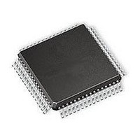
ST72T511R9T6 STMicroelectronics, ST72T511R9T6 Datasheet - Page 110

ST72T511R9T6
Manufacturer Part Number
ST72T511R9T6
Description
Microcontrollers (MCU) UV EPROM 60K SPI/SCI
Manufacturer
STMicroelectronics
Datasheet
1.ST72T511R9T6.pdf
(164 pages)
Specifications of ST72T511R9T6
Data Bus Width
8 bit
Program Memory Type
EEPROM
Program Memory Size
60 KB
Data Ram Size
2048 B
Interface Type
CAN, SCI, SPI
Maximum Clock Frequency
8 MHz
Number Of Programmable I/os
48
Number Of Timers
5
Operating Supply Voltage
3 V to 5.5 V
Maximum Operating Temperature
+ 85 C
Mounting Style
SMD/SMT
Package / Case
TQFP-64
Minimum Operating Temperature
- 40 C
On-chip Adc
8 bit
Lead Free Status / Rohs Status
No
Available stocks
Company
Part Number
Manufacturer
Quantity
Price
- Current page: 110 of 164
- Download datasheet (2Mb)
ST72311R, ST72511R, ST72512R, ST72532R
CONTROLLER AREA NETWORK (Cont’d)
10.7.3.4 Bit Timing Logic
The bit timing logic monitors the serial bus-line and
performs sampling and adjustment of the sample
point by synchronizing on the start-bit edge and re-
synchronizing on following edges.
Its operation may be explained simply when the
nominal bit time is divided into three segments as
follows:
– Synchronisation segment (SYNC_SEG): a bit
– Bit segment 1 (BS1): defines the location of the
– Bit segment 2 (BS2): defines the location of the
Figure 59. Bit Timing
110/164
change is expected to lie within this time seg-
ment. It has a fixed length of one time quanta (1
x t
sample point. It includes the PROP_SEG and
PHASE_SEG1 of the CAN standard. Its duration
is programmable between 1 and 16 time quanta
but may be automatically lengthened to compen-
sate for positive phase drifts due to differences in
the frequency of the various nodes of the net-
work.
transmit point. It represents the PHASE_SEG2
of the CAN standard. Its duration is programma-
ble between 1 and 8 time quanta but may also be
automatically shortened to compensate for neg-
ative phase drifts.
CAN
).
SYNC_SEG
1 x t
CAN
BIT SEGMENT 1 (BS1)
t
BS1
NOMINAL BIT TIME
The resynchronization jump width (RJW) defines
an upper bound to the amount of lengthening or
shortening of the bit segments. It is programmable
between 1 and 4 time quanta.
A valid edge is defined as the first transition in a bit
time from dominant to recessive bus level provid-
ed the controller itself does not send a recessive
bit.
If a valid edge is detected in BS1 instead of
SYNC_SEG, BS1 is extended by up to RJW so
that the sample point is delayed.
Conversely, if a valid edge is detected in BS2 in-
stead of SYNC_SEG, BS2 is shortened by up to
RJW so that the transmit point is moved earlier.
As a safeguard against programming errors, the
configuration of the Bit Timing Register (BTR) is
only possible while the device is in STANDBY
mode.
SAMPLE POINT
BIT SEGMENT 2 (BS2)
t
BS2
TRANS MIT POINT
Related parts for ST72T511R9T6
Image
Part Number
Description
Manufacturer
Datasheet
Request
R

Part Number:
Description:
STMicroelectronics [RIPPLE-CARRY BINARY COUNTER/DIVIDERS]
Manufacturer:
STMicroelectronics
Datasheet:

Part Number:
Description:
STMicroelectronics [LIQUID-CRYSTAL DISPLAY DRIVERS]
Manufacturer:
STMicroelectronics
Datasheet:

Part Number:
Description:
BOARD EVAL FOR MEMS SENSORS
Manufacturer:
STMicroelectronics
Datasheet:

Part Number:
Description:
NPN TRANSISTOR POWER MODULE
Manufacturer:
STMicroelectronics
Datasheet:

Part Number:
Description:
TURBOSWITCH ULTRA-FAST HIGH VOLTAGE DIODE
Manufacturer:
STMicroelectronics
Datasheet:

Part Number:
Description:
Manufacturer:
STMicroelectronics
Datasheet:

Part Number:
Description:
DIODE / SCR MODULE
Manufacturer:
STMicroelectronics
Datasheet:

Part Number:
Description:
DIODE / SCR MODULE
Manufacturer:
STMicroelectronics
Datasheet:

Part Number:
Description:
Search -----> STE16N100
Manufacturer:
STMicroelectronics
Datasheet:

Part Number:
Description:
Search ---> STE53NA50
Manufacturer:
STMicroelectronics
Datasheet:

Part Number:
Description:
NPN Transistor Power Module
Manufacturer:
STMicroelectronics
Datasheet:

Part Number:
Description:
DIODE / SCR MODULE
Manufacturer:
STMicroelectronics
Datasheet:


