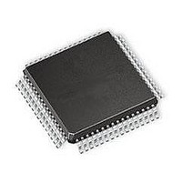
ST72T511R9T6 STMicroelectronics, ST72T511R9T6 Datasheet - Page 143

ST72T511R9T6
Manufacturer Part Number
ST72T511R9T6
Description
Microcontrollers (MCU) UV EPROM 60K SPI/SCI
Manufacturer
STMicroelectronics
Datasheet
1.ST72T511R9T6.pdf
(164 pages)
Specifications of ST72T511R9T6
Data Bus Width
8 bit
Program Memory Type
EEPROM
Program Memory Size
60 KB
Data Ram Size
2048 B
Interface Type
CAN, SCI, SPI
Maximum Clock Frequency
8 MHz
Number Of Programmable I/os
48
Number Of Timers
5
Operating Supply Voltage
3 V to 5.5 V
Maximum Operating Temperature
+ 85 C
Mounting Style
SMD/SMT
Package / Case
TQFP-64
Minimum Operating Temperature
- 40 C
On-chip Adc
8 bit
Lead Free Status / Rohs Status
No
Available stocks
Company
Part Number
Manufacturer
Quantity
Price
- Current page: 143 of 164
- Download datasheet (2Mb)
EMC CHARACTERISTICS (Cont’d)
12.7.3 ESD Pin Protection Strategy
To protect an integrated circuit against Electro-
Static Discharge the stress must be controlled to
prevent degradation or destruction of the circuit el-
ements. The stress generally affects the circuit el-
ements which are connected to the pads but can
also affect the internal devices when the supply
pads receive the stress. The elements to be pro-
tected must not receive excessive current, voltage
or heating within their structure.
An ESD network combines the different input and
output ESD protections. This network works, by al-
lowing safe discharge paths for the pins subjected
to ESD stress. Two critical ESD stress cases are
presented in Figure 77 and Figure 78 for standard
pins and in Figure 79 and Figure 80 for true open
drain pins.
Figure 77. Positive Stress on a Standard Pad vs. V
Figure 78. Negative Stress on a Standard Pad vs. V
Main path
Path to avoid
Main path
V
V
V
V
DD
DD
SS
SS
(3a)
(3b)
(3a)
(3b)
OUT
OUT
ST72311R, ST72511R, ST72512R, ST72532R
SS
Standard Pin Protection
To protect the output structure the following ele-
ments are added:
To protect the input structure the following ele-
ments are added:
DD
– A diode to V
– A protection device between V
– A resistor in series with the pad (1)
– A diode to V
– A protection device between V
(4)
(4)
IN
IN
DD
DD
(3a) and a diode from V
(2a) and a diode from V
(2a)
(2b)
(2a)
(2b)
(1)
(1)
DD
DD
and V
and V
143/164
SS
SS
SS
SS
V
V
V
V
DD
SS
DD
SS
(3b)
(2b)
(4)
(4)
Related parts for ST72T511R9T6
Image
Part Number
Description
Manufacturer
Datasheet
Request
R

Part Number:
Description:
STMicroelectronics [RIPPLE-CARRY BINARY COUNTER/DIVIDERS]
Manufacturer:
STMicroelectronics
Datasheet:

Part Number:
Description:
STMicroelectronics [LIQUID-CRYSTAL DISPLAY DRIVERS]
Manufacturer:
STMicroelectronics
Datasheet:

Part Number:
Description:
BOARD EVAL FOR MEMS SENSORS
Manufacturer:
STMicroelectronics
Datasheet:

Part Number:
Description:
NPN TRANSISTOR POWER MODULE
Manufacturer:
STMicroelectronics
Datasheet:

Part Number:
Description:
TURBOSWITCH ULTRA-FAST HIGH VOLTAGE DIODE
Manufacturer:
STMicroelectronics
Datasheet:

Part Number:
Description:
Manufacturer:
STMicroelectronics
Datasheet:

Part Number:
Description:
DIODE / SCR MODULE
Manufacturer:
STMicroelectronics
Datasheet:

Part Number:
Description:
DIODE / SCR MODULE
Manufacturer:
STMicroelectronics
Datasheet:

Part Number:
Description:
Search -----> STE16N100
Manufacturer:
STMicroelectronics
Datasheet:

Part Number:
Description:
Search ---> STE53NA50
Manufacturer:
STMicroelectronics
Datasheet:

Part Number:
Description:
NPN Transistor Power Module
Manufacturer:
STMicroelectronics
Datasheet:

Part Number:
Description:
DIODE / SCR MODULE
Manufacturer:
STMicroelectronics
Datasheet:


