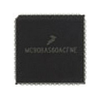
MC68HC11E1CFN3R2 Freescale Semiconductor, MC68HC11E1CFN3R2 Datasheet - Page 44

MC68HC11E1CFN3R2
Manufacturer Part Number
MC68HC11E1CFN3R2
Description
Manufacturer
Freescale Semiconductor
Datasheet
1.MC68HC11E1CFN3R2.pdf
(242 pages)
Specifications of MC68HC11E1CFN3R2
Cpu Family
HC11
Device Core Size
8b
Frequency (max)
3MHz
Interface Type
SCI/SPI
Program Memory Type
ROMLess
Program Memory Size
Not Required
Total Internal Ram Size
512Byte
# I/os (max)
38
Number Of Timers - General Purpose
8
Operating Supply Voltage (typ)
3.3/5V
Operating Supply Voltage (max)
5.5V
Operating Supply Voltage (min)
3V
On-chip Adc
8-chx8-bit
Instruction Set Architecture
CISC
Operating Temp Range
-40C to 85C
Operating Temperature Classification
Industrial
Mounting
Surface Mount
Pin Count
52
Package Type
PLCC
Lead Free Status / Rohs Status
Not Compliant
- Current page: 44 of 242
- Download datasheet (2Mb)
Operating Modes and On-Chip Memory
EE[3:0] — EEPROM Mapping Bits
44
EE[3:0] apply only to MC68HC811E2 and allow the 2048 bytes of EEPROM to be remapped to any
4-Kbyte boundary. See
Resets:
U indicates a previously programmed bit. U(L) indicates that the bit resets to the logic level held in the latch prior to reset,
but the function of COP is controlled by the DISR bit in TEST1 register.
Single chip:
Expanded:
Bootstrap:
Address:
Figure 2-11. MC68HC811E2 System Configuration Register (CONFIG)
Read:
Write:
Test:
$103F
Bit 7
EE3
U
U
1
1
Table
= Unimplemented
2-3.
EE2
EE[3:0]
U
U
6
1
1
0 0 0 0
0 0 0 1
0 0 1 0
0 0 1 1
0 1 0 0
0 1 0 1
0 1 1 0
0 1 1 1
1 0 0 0
1 0 0 1
1 0 1 0
1 0 1 1
1 1 0 0
1 1 0 1
1 1 1 0
1 1 1 1
M68HC11E Family Data Sheet, Rev. 5.1
Table 2-3. EEPROM Mapping
EE1
U
U
5
1
1
EE0
U
U
4
1
1
EEPROM Location
$C800–$CFFF
$D800–$DFFF
$A800–$AFFF
$B800–$BFFF
$E800–$EFFF
$F800–$FFFF
$0800–$0FFF
$1800–$1FFF
$2800–$2FFF
$3800–$3FFF
$4800–$4FFF
$5800–$5FFF
$6800–$6FFF
$7800–$7FFF
$8800–$8FFF
$9800–$9FFF
NOSEC
U
U
3
1
1
NOCOP
U(L)
U(L)
U
U
2
1
1
1
1
1
Freescale Semiconductor
EEON
Bit 0
U
1
1
0
Related parts for MC68HC11E1CFN3R2
Image
Part Number
Description
Manufacturer
Datasheet
Request
R
Part Number:
Description:
Manufacturer:
Freescale Semiconductor, Inc
Datasheet:
Part Number:
Description:
Manufacturer:
Freescale Semiconductor, Inc
Datasheet:
Part Number:
Description:
Manufacturer:
Freescale Semiconductor, Inc
Datasheet:
Part Number:
Description:
Manufacturer:
Freescale Semiconductor, Inc
Datasheet:
Part Number:
Description:
Manufacturer:
Freescale Semiconductor, Inc
Datasheet:
Part Number:
Description:
Manufacturer:
Freescale Semiconductor, Inc
Datasheet:
Part Number:
Description:
Manufacturer:
Freescale Semiconductor, Inc
Datasheet:
Part Number:
Description:
Manufacturer:
Freescale Semiconductor, Inc
Datasheet:
Part Number:
Description:
Manufacturer:
Freescale Semiconductor, Inc
Datasheet:
Part Number:
Description:
Manufacturer:
Freescale Semiconductor, Inc
Datasheet:
Part Number:
Description:
Manufacturer:
Freescale Semiconductor, Inc
Datasheet:
Part Number:
Description:
Manufacturer:
Freescale Semiconductor, Inc
Datasheet:
Part Number:
Description:
Manufacturer:
Freescale Semiconductor, Inc
Datasheet:
Part Number:
Description:
Manufacturer:
Freescale Semiconductor, Inc
Datasheet:
Part Number:
Description:
Manufacturer:
Freescale Semiconductor, Inc
Datasheet:


