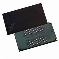
MT48V8M16LFB4-8:G Micron Technology Inc, MT48V8M16LFB4-8:G Datasheet - Page 16

MT48V8M16LFB4-8:G
Manufacturer Part Number
MT48V8M16LFB4-8:G
Description
IC SDRAM 128MBIT 125MHZ 54VFBGA
Manufacturer
Micron Technology Inc
Type
Mobile SDRAMr
Specifications of MT48V8M16LFB4-8:G
Format - Memory
RAM
Memory Type
Mobile SDRAM
Memory Size
128M (8Mx16)
Speed
125MHz
Interface
Parallel
Voltage - Supply
2.3 V ~ 2.7 V
Operating Temperature
0°C ~ 70°C
Package / Case
54-VFBGA
Organization
8Mx16
Density
128Mb
Address Bus
14b
Access Time (max)
19/8/7ns
Maximum Clock Rate
125MHz
Operating Supply Voltage (typ)
2.5V
Package Type
VFBGA
Operating Temp Range
0C to 70C
Operating Supply Voltage (max)
2.7V
Operating Supply Voltage (min)
2.3V
Supply Current
100mA
Pin Count
54
Mounting
Surface Mount
Operating Temperature Classification
Commercial
Lead Free Status / RoHS Status
Lead free / RoHS Compliant
Available stocks
Company
Part Number
Manufacturer
Quantity
Price
Company:
Part Number:
MT48V8M16LFB4-8:G
Manufacturer:
MICRON
Quantity:
4 000
Company:
Part Number:
MT48V8M16LFB4-8:G
Manufacturer:
Micron Technology Inc
Quantity:
10 000
Company:
Part Number:
MT48V8M16LFB4-8:G TR
Manufacturer:
Micron Technology Inc
Quantity:
10 000
Register Definition
Mode Register
PDF: 09005aef807f4885/Source: 09005aef8071a76b
128Mbx16x32Mobile_2.fm - Rev. M 1/09 EN
Note:
10. Issue an AUTO REFRESH command.
11. Wait at least
12. The SDRAM is now ready for mode register programming. Because the mode register
13. Wait at least
14. Using the LMR command, program the extended mode register. The low-power
15. Wait at least
7. Wait at least
8. Issue an AUTO REFRESH command.
9. Wait at least
At this point, the DRAM is ready for any valid command.
To achieve low power consumption, there are two mode registers in the Mobile compo-
nent: mode register and extended mode register. Mode register is discussed in this
section. Extended mode register is discussed on page 21. The mode register is used to
define the specific mode of operation of the SDRAM. This definition includes the selec-
tion of BL, a burst type, CL, an operating mode, and a write burst mode, as shown in
Figure 7 on page 18. The mode register is programmed via the LOAD MODE REGISTER
command and will retain the stored information until it is programmed again or the
device loses power.
Mode register bits M0–M2 specify BL, M3 specifies the type of burst (sequential or inter-
leaved), M4–M6 specify CL, M7 and M8 specify the operating mode, M9 specify the write
burst mode (single or programmed burst length), M10 and M11 are reserved and must
be set to zero. To address the mode register, M12 and M13 must be set to zero.
given. All banks will complete their precharge, thereby placing the device in the all
banks idle state.
are allowed.
are allowed.
will power up in an unknown state, it should be loaded with desired bit values prior to
applying any operational command. Using the LMR command, program the mode
register. The mode register is programmed via the MODE REGISTER SET command
with BA1 = 0, BA0 = 0 and retains the stored information until it is programmed again
or the device loses power. Not programming the mode register upon initialization will
result in default settings, which may not be desired. Outputs are guaranteed High-Z
after the LMR command is issued. Outputs should be High-Z already before the LMR
command is issued.
allowed.
extended mode register is programmed via the MODE REGISTER SET command with
BA1 = 1, BA0 = 0 and retains the stored information until it is programmed again or
the device loses power. Not programming the extended mode register upon initializa-
tion will result in default settings for the low-power features. The extended mode will
default with the temperature sensor enabled, full drive strength, and full array refresh.
allowed.
If desired, more than two AUTO REFRESH commands can be issued in the sequence.
After steps 9 and 10 are complete, repeat them until the desired number of AUTO
REFRESH +
t
t
t
t
t
t
RFC loops is achieved.
RP time; during this time, NOPs or DESELECT commands must be
RFC time, during which only NOPs or COMMAND INHIBIT commands
RFC time, during which only NOPs or COMMAND INHIBIT commands
MRD time, during which only NOP or DESELECT commands are
MRD time, during which only NOP or DESELECT commands are
16
Micron Technology, Inc., reserves the right to change products or specifications without notice.
128Mb: x16, x32 Mobile SDRAM
©2001 Micron Technology, Inc. All rights reserved.
Register Definition


