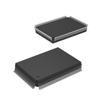
D12350F20IV Renesas Electronics America, D12350F20IV Datasheet - Page 171

D12350F20IV
Manufacturer Part Number
D12350F20IV
Description
IC H8S/2350 MCU 4.5/5.5V 0+K I-T
Manufacturer
Renesas Electronics America
Series
H8® H8S/2300r
Specifications of D12350F20IV
Core Processor
H8S/2000
Core Size
16-Bit
Speed
20MHz
Connectivity
SCI, SmartCard
Peripherals
DMA, POR, PWM, WDT
Number Of I /o
87
Program Memory Type
ROMless
Ram Size
2K x 8
Voltage - Supply (vcc/vdd)
2.7 V ~ 5.5 V
Data Converters
A/D 8x10b; D/A 2x8b
Oscillator Type
Internal
Operating Temperature
-40°C ~ 85°C
Package / Case
128-QFP
Lead Free Status / RoHS Status
Lead free / RoHS Compliant
Eeprom Size
-
Program Memory Size
-
Available stocks
Company
Part Number
Manufacturer
Quantity
Price
Company:
Part Number:
D12350F20IV
Manufacturer:
INF
Quantity:
4 834
- Current page: 171 of 1027
- Download datasheet (6Mb)
Bit 3—DACK Timing Select (DDS): Selects the DMAC single address transfer bus timing for
the DRAM interface.
Bit 2—Reserved: Only 1 should be written to this bit.
Bit 1—Write Data Buffer Enable (WDBE): Selects whether or not the write buffer function is
used for an external write cycle or DMAC single address cycle.
Bit 0—WAIT Pin Enable (WAITE): Selects enabling or disabling of wait input by the WAIT
pin.
Bit 3
DDS
0
1
Bit 1
WDBE
0
1
Bit 0
WAITE
0
1
Description
When DMAC single address transfer is performed in DRAM space, full access is
always executed
DACK signal goes low from T
Burst access is possible when DMAC single address transfer is performed in DRAM
space
DACK signal goes low from T
Description
Write data buffer function not used
Write data buffer function used
Description
Wait input by WAIT pin disabled. WAIT pin can be used as I/O port.
Wait input by WAIT pin enabled
r
c1
or T
or T
1
2
cycle
cycle
Rev. 3.00 Sep 15, 2006 page 135 of 988
Section 6 Bus Controller
REJ09B0330-0300
(Initial value)
(Initial value)
(Initial value)
Related parts for D12350F20IV
Image
Part Number
Description
Manufacturer
Datasheet
Request
R

Part Number:
Description:
KIT STARTER FOR M16C/29
Manufacturer:
Renesas Electronics America
Datasheet:

Part Number:
Description:
KIT STARTER FOR R8C/2D
Manufacturer:
Renesas Electronics America
Datasheet:

Part Number:
Description:
R0K33062P STARTER KIT
Manufacturer:
Renesas Electronics America
Datasheet:

Part Number:
Description:
KIT STARTER FOR R8C/23 E8A
Manufacturer:
Renesas Electronics America
Datasheet:

Part Number:
Description:
KIT STARTER FOR R8C/25
Manufacturer:
Renesas Electronics America
Datasheet:

Part Number:
Description:
KIT STARTER H8S2456 SHARPE DSPLY
Manufacturer:
Renesas Electronics America
Datasheet:

Part Number:
Description:
KIT STARTER FOR R8C38C
Manufacturer:
Renesas Electronics America
Datasheet:

Part Number:
Description:
KIT STARTER FOR R8C35C
Manufacturer:
Renesas Electronics America
Datasheet:

Part Number:
Description:
KIT STARTER FOR R8CL3AC+LCD APPS
Manufacturer:
Renesas Electronics America
Datasheet:

Part Number:
Description:
KIT STARTER FOR RX610
Manufacturer:
Renesas Electronics America
Datasheet:

Part Number:
Description:
KIT STARTER FOR R32C/118
Manufacturer:
Renesas Electronics America
Datasheet:

Part Number:
Description:
KIT DEV RSK-R8C/26-29
Manufacturer:
Renesas Electronics America
Datasheet:

Part Number:
Description:
KIT STARTER FOR SH7124
Manufacturer:
Renesas Electronics America
Datasheet:

Part Number:
Description:
KIT STARTER FOR H8SX/1622
Manufacturer:
Renesas Electronics America
Datasheet:

Part Number:
Description:
KIT DEV FOR SH7203
Manufacturer:
Renesas Electronics America
Datasheet:


