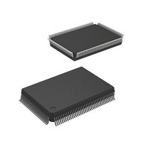
D12350F20IV Renesas Electronics America, D12350F20IV Datasheet - Page 53

D12350F20IV
Manufacturer Part Number
D12350F20IV
Description
IC H8S/2350 MCU 4.5/5.5V 0+K I-T
Manufacturer
Renesas Electronics America
Series
H8® H8S/2300r
Specifications of D12350F20IV
Core Processor
H8S/2000
Core Size
16-Bit
Speed
20MHz
Connectivity
SCI, SmartCard
Peripherals
DMA, POR, PWM, WDT
Number Of I /o
87
Program Memory Type
ROMless
Ram Size
2K x 8
Voltage - Supply (vcc/vdd)
2.7 V ~ 5.5 V
Data Converters
A/D 8x10b; D/A 2x8b
Oscillator Type
Internal
Operating Temperature
-40°C ~ 85°C
Package / Case
128-QFP
Lead Free Status / RoHS Status
Lead free / RoHS Compliant
Eeprom Size
-
Program Memory Size
-
Available stocks
Company
Part Number
Manufacturer
Quantity
Price
Company:
Part Number:
D12350F20IV
Manufacturer:
INF
Quantity:
4 834
- Current page: 53 of 1027
- Download datasheet (6Mb)
Type
Bus control
DMA controller
(DMAC)
16-bit timer-
pulse unit
(TPU)
Symbol
CAS
LCAS
WAIT
DREQ1,
DREQ0
TEND1,
TEND0
DACK1,
DACK0
TCLKD to
TCLKA
TIOCA0,
TIOCB0,
TIOCC0,
TIOCD0
TIOCA1,
TIOCB1
TIOCA2,
TIOCB2
TFP-120
116
86
86
62, 60
63, 61
111, 112
105, 107,
109, 110
112 to
109
108, 107
106, 105
Pin No.
FP-128
126
94
94
70, 66
71, 69
121, 122
115, 117,
119, 120
122 to
119
118, 117
116, 115
I/O
Output Upper column address
Output Lower column address strobe: The 2-
Input
Input
Output DMA transfer end 1 and 0: These
Output DMA transfer acknowledge 1 and 0:
Input
I/O
I/O
I/O
Rev. 3.00 Sep 15, 2006 page 17 of 988
Name and Function
strobe/column address strobe:
The 2CAS type DRAM upper column
address strobe signal.
CAS type DRAM lower column
address strobe signal
Wait: Requests insertion of a wait
state in the bus cycle when
accessing external 3-state address
space.
DMA request 1 and 0: These pins
request DMAC activation.
pins indicate the end of DMAC data
transfer.
These are the DMAC single address
transfer acknowledge pins.
Clock input D to A: These pins input
an external clock.
Input capture/ output compare match
A0 to D0: The TGR0A to TGR0D
input capture input or output
compare output, or PWM output pins.
Input capture/ output compare match
A1 and B1: The TGR1A and TGR1B
input capture input or output
compare output, or PWM output pins.
Input capture/ output compare match
A2 and B2: The TGR2A and TGR2B
input capture input or output
compare output, or PWM output pins.
Section 1 Overview
REJ09B0330-0300
Related parts for D12350F20IV
Image
Part Number
Description
Manufacturer
Datasheet
Request
R

Part Number:
Description:
KIT STARTER FOR M16C/29
Manufacturer:
Renesas Electronics America
Datasheet:

Part Number:
Description:
KIT STARTER FOR R8C/2D
Manufacturer:
Renesas Electronics America
Datasheet:

Part Number:
Description:
R0K33062P STARTER KIT
Manufacturer:
Renesas Electronics America
Datasheet:

Part Number:
Description:
KIT STARTER FOR R8C/23 E8A
Manufacturer:
Renesas Electronics America
Datasheet:

Part Number:
Description:
KIT STARTER FOR R8C/25
Manufacturer:
Renesas Electronics America
Datasheet:

Part Number:
Description:
KIT STARTER H8S2456 SHARPE DSPLY
Manufacturer:
Renesas Electronics America
Datasheet:

Part Number:
Description:
KIT STARTER FOR R8C38C
Manufacturer:
Renesas Electronics America
Datasheet:

Part Number:
Description:
KIT STARTER FOR R8C35C
Manufacturer:
Renesas Electronics America
Datasheet:

Part Number:
Description:
KIT STARTER FOR R8CL3AC+LCD APPS
Manufacturer:
Renesas Electronics America
Datasheet:

Part Number:
Description:
KIT STARTER FOR RX610
Manufacturer:
Renesas Electronics America
Datasheet:

Part Number:
Description:
KIT STARTER FOR R32C/118
Manufacturer:
Renesas Electronics America
Datasheet:

Part Number:
Description:
KIT DEV RSK-R8C/26-29
Manufacturer:
Renesas Electronics America
Datasheet:

Part Number:
Description:
KIT STARTER FOR SH7124
Manufacturer:
Renesas Electronics America
Datasheet:

Part Number:
Description:
KIT STARTER FOR H8SX/1622
Manufacturer:
Renesas Electronics America
Datasheet:

Part Number:
Description:
KIT DEV FOR SH7203
Manufacturer:
Renesas Electronics America
Datasheet:


