QB-MINI2-EE NEC, QB-MINI2-EE Datasheet - Page 21
QB-MINI2-EE
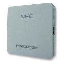
Manufacturer Part Number
QB-MINI2-EE
Description
EMULATOR, PROGRAMMER, MINICUBE2
Manufacturer
NEC
Type
Debug Emulatorr
Datasheet
1.QB-MINI2-EE.pdf
(169 pages)
Specifications of QB-MINI2-EE
Svhc
No SVHC (18-Jun-2010)
Mcu Supported Families
MINICUBE2
Silicon Family Name
V850, 78K0R, 78K0S
Ic Product Type
On-Chip Debug Emulator
Kit Contents
MINICUBE2, USB Cable, Target Cable, 78K0-OCD Board
Features
On-Chip Debugging, Flash Memory Programming,


Notes 1. Connect TxD (transmit side) of the target device to RxD (receive side) of the target connector, and TxD
Target connector
Target connector
RESET_IN
RESET_IN
Figure 3-2. Recommended Circuit Connection When UART Is Used for Communication Interface
RESET_OUT
RESET_OUT
2. This pin may be used to supply an external clock during flash programming (4, 8 or 16 MHz). For the
3. The alternate function of this pin can be used because this pin goes to Hi-Z when debugging.
4. This connection is designed assuming that the RESET signal is output from the N-ch open-drain buffer
5. The circuit enclosed by a dashed line is not required when only flash programming is performed.
6. The circuit enclosed by a dashed line is designed for flash self programming, which controls the FLMD0
FLMD1
FLMD1
FLMD0
FLMD0
RXD
RXD
(transmit side) of the target connector to RxD (receive side) of the target device. Read the serial interface
pin names on the target device side as those for flash programming supported by the target device.
connection, refer to the user's manual for the target device.
(output resistance: 100Ω or less). For details, refer to 3.1.3 Connection of reset pin.
pin via ports. Use the port for inputting or outputting the high level. When flash self programming is not
performed, a pull-down resistance for the FLMD0 pin can be within 1 to 10 kΩ.
TXD
TXD
CLK
CLK
R.F.U.
R.F.U.
R.F.U.
R.F.U.
R.F.U.
R.F.U.
R.F.U.
R.F.U.
R.F.U.
R.F.U.
R.F.U.
R.F.U.
R.F.U.
R.F.U.
GND
GND
Note 1
Note 1
Note 1
Note 1
Note 2
Note 2
Note 3
Note 3
Note 4
Note 4
VDD
VDD
Note 3
Note 3
1
1
2
2
3
3
4
4
5
5
6
6
7
7
8
8
9
9
10
10
11
11
12
12
13
13
14
14
15
15
16
16
CHAPTER 3
V
V
DD
DD
Note 5
Note 5
10 kΩ
10 kΩ
HOW TO USE MINICUBE2 WITH V850 MICROCONTROLLER
1 kΩ
1 kΩ
User’s Manual U18371EJ1V0UM
V
V
DD
DD
1 to 10 kΩ
1 to 10 kΩ
1 to 10 kΩ
1 to 10 kΩ
V
V
DD
DD
3 to 10 kΩ
3 to 10 kΩ
10 kΩ
10 kΩ
V
V
DD
DD
100 Ω
100 Ω
GND
GND
_RESET
_RESET
TXD
TXD
VDD
VDD
RXD
RXD
FLMD1
FLMD1
FLMD0
FLMD0
Port X
Port X
Reset connector
Reset connector
Target device
Target device
RESET signal
RESET signal
Note 6
Note 6
X1
X1
X2
X2
Clock
Clock
circuit
circuit
21
Related parts for QB-MINI2-EE
Image
Part Number
Description
Manufacturer
Datasheet
Request
R

Part Number:
Description:
16/8 bit single-chip microcomputer
Manufacturer:
NEC
Datasheet:
Part Number:
Description:
Dual audio power amp circuit
Manufacturer:
NEC
Datasheet:
Part Number:
Description:
Dual comparator
Manufacturer:
NEC
Datasheet:
Part Number:
Description:
MOS type composite field effect transistor
Manufacturer:
NEC
Datasheet:
Part Number:
Description:
50 V/100 mA FET array incorporating 2 N-ch MOSFETs
Manufacturer:
NEC
Datasheet:
Part Number:
Description:
6-pin small MM high-frequency double transistor
Manufacturer:
NEC
Datasheet:
Part Number:
Description:
6-pin small MM high-frequency double transistor
Manufacturer:
NEC
Datasheet:
Part Number:
Description:
6-pin small MM high-frequency double transistor
Manufacturer:
NEC
Datasheet:
Part Number:
Description:
6-pin small MM high-frequency double transistor
Manufacturer:
NEC
Datasheet:
Part Number:
Description:
Twin transistors equipped with different model chips(6P small MM)
Manufacturer:
NEC
Datasheet:
Part Number:
Description:
Bipolar analog integrated circuit
Manufacturer:
NEC
Datasheet: