QB-MINI2-EE NEC, QB-MINI2-EE Datasheet - Page 69
QB-MINI2-EE
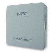
Manufacturer Part Number
QB-MINI2-EE
Description
EMULATOR, PROGRAMMER, MINICUBE2
Manufacturer
NEC
Type
Debug Emulatorr
Datasheet
1.QB-MINI2-EE.pdf
(169 pages)
Specifications of QB-MINI2-EE
Svhc
No SVHC (18-Jun-2010)
Mcu Supported Families
MINICUBE2
Silicon Family Name
V850, 78K0R, 78K0S
Ic Product Type
On-Chip Debug Emulator
Kit Contents
MINICUBE2, USB Cable, Target Cable, 78K0-OCD Board
Features
On-Chip Debugging, Flash Memory Programming,


4.1.4 Cautions on target system design
• Do not place X1/OCD1A and X2/OCD1B next to each other on the target system.
• Make the distance between the target connector and the target device as short as possible.
• Since the X1/OCD1A and X2/OCD1B lines are used for clock supply, be sure to shield them, such as with a
• Before shipping the product, use jumpers or other means to physically separate the X1/OCD1A and X2/OCD1B
• When debugging, remove capacitors, feedback resistors, and other elements for the resonator in order to
they should be made as short as possible.
GND pattern.
pins from the target connector in order to ensure normal clock oscillation.
prevent signal degradation due to the load placed on the X1/OCD1A and X2/OCD1B pins.
Note the following cautions when designing the target system.
GND pattern
GND pattern
Target device
Target device
CHAPTER 4
X1
X1
Figure 4-19. Reference Diagram of Target System
X2
X2
HOW TO USE MINICUBE2 WITH 78K0 MICROCONTROLLER
User’s Manual U18371EJ1V0UM
Make the pattern where X1 and X2 are
Make the pattern where X1 and X2 are
next to each other as short as possible, or
next to each other as short as possible, or
make the space wider
make the space wider
Connect to the connector by using
Connect to the connector by using
tin plating when debugging
tin plating when debugging
Shield both sides of the line to
Shield both sides of the line to
reduce noise
reduce noise
If the layout requires this,
To debug
To debug
connector
connector
69
Related parts for QB-MINI2-EE
Image
Part Number
Description
Manufacturer
Datasheet
Request
R

Part Number:
Description:
16/8 bit single-chip microcomputer
Manufacturer:
NEC
Datasheet:
Part Number:
Description:
Dual audio power amp circuit
Manufacturer:
NEC
Datasheet:
Part Number:
Description:
Dual comparator
Manufacturer:
NEC
Datasheet:
Part Number:
Description:
MOS type composite field effect transistor
Manufacturer:
NEC
Datasheet:
Part Number:
Description:
50 V/100 mA FET array incorporating 2 N-ch MOSFETs
Manufacturer:
NEC
Datasheet:
Part Number:
Description:
6-pin small MM high-frequency double transistor
Manufacturer:
NEC
Datasheet:
Part Number:
Description:
6-pin small MM high-frequency double transistor
Manufacturer:
NEC
Datasheet:
Part Number:
Description:
6-pin small MM high-frequency double transistor
Manufacturer:
NEC
Datasheet:
Part Number:
Description:
6-pin small MM high-frequency double transistor
Manufacturer:
NEC
Datasheet:
Part Number:
Description:
Twin transistors equipped with different model chips(6P small MM)
Manufacturer:
NEC
Datasheet:
Part Number:
Description:
Bipolar analog integrated circuit
Manufacturer:
NEC
Datasheet: