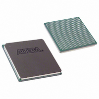
EP1S10F780I6N Altera, EP1S10F780I6N Datasheet - Page 242

EP1S10F780I6N
Manufacturer Part Number
EP1S10F780I6N
Description
IC STRATIX FPGA 10K LE 780-FBGA
Manufacturer
Altera
Series
Stratix®r
Datasheet
1.EP1S10F484I6N.pdf
(864 pages)
Specifications of EP1S10F780I6N
Number Of Logic Elements/cells
10570
Number Of Labs/clbs
1057
Total Ram Bits
920448
Number Of I /o
426
Voltage - Supply
1.425 V ~ 1.575 V
Mounting Type
Surface Mount
Operating Temperature
0°C ~ 85°C
Package / Case
780-FBGA
Lead Free Status / RoHS Status
Lead free / RoHS Compliant
Number Of Gates
-
Available stocks
Company
Part Number
Manufacturer
Quantity
Price
Company:
Part Number:
EP1S10F780I6N
Manufacturer:
ALTERA
Quantity:
3 000
- Current page: 242 of 864
- Download datasheet (11Mb)
Timing Model
4–62
Stratix Device Handbook, Volume 1
3.3-V LVTTL
2.5-V LVTTL
1.8-V LVTTL
1.5-V LVTTL
3.3-V LVCMOS
2.5-V LVCMOS
1.8-V LVCMOS
1.5-V LVCMOS
3.3-V GTL
2.5-V GTL
3.3-V GTL+
2.5-V GTL+
3.3-V SSTL-3 Class II
Table 4–101. Reporting Methodology For Maximum Timing For Single-Ended Output Pins (Part 1 of 2)
Notes
I/O Standard
(1), (2),
(3)
R
Figure 4–7. Output Delay Timing Reporting Setup Modeled by Quartus II
Notes to
(1)
(2)
–
–
–
–
–
–
–
–
–
–
–
–
–
UP
Output pin timing is reported at the output pin of the FPGA device. Additional
delays for loading and board trace delay need to be accounted for with IBIS model
simulations.
V
CCINT
R
Figure
–
–
–
–
–
–
–
–
–
–
–
–
–
DN
is 1.42-V unless otherwise specified.
4–7:
Loading and Termination
R
25
0
0
0
0
0
0
0
0
0
0
0
0
S
VCCIO
Output
Buffer
GND
25
25
25
25
25
R
–
–
–
–
–
–
–
–
T
Single-Ended Outputs
OUTPUT
2.950
2.370
1.650
1.400
2.950
2.370
1.650
1.400
2.950
2.370
2.950
2.370
2.950
V
(V)
CCIO
V
MEAS
VCCIO
GND
2.95
2.37
1.65
1.40
2.95
2.37
1.65
1.40
1.14
1.14
1.35
1.35
1.25
VTT
(V)
R
R
DN
UP
R
S
GND
V
TT
(pF)
C
R
10
10
10
10
10
10
10
10
30
30
30
30
30
C
L
T
L
Altera Corporation
Measurement
January 2006
V
1.500
1.200
0.880
0.750
1.500
1.200
0.880
0.750
0.740
0.740
0.880
0.880
1.250
Point
MEAS
Related parts for EP1S10F780I6N
Image
Part Number
Description
Manufacturer
Datasheet
Request
R

Part Number:
Description:
CYCLONE II STARTER KIT EP2C20N
Manufacturer:
Altera
Datasheet:

Part Number:
Description:
CPLD, EP610 Family, ECMOS Process, 300 Gates, 16 Macro Cells, 16 Reg., 16 User I/Os, 5V Supply, 35 Speed Grade, 24DIP
Manufacturer:
Altera Corporation
Datasheet:

Part Number:
Description:
CPLD, EP610 Family, ECMOS Process, 300 Gates, 16 Macro Cells, 16 Reg., 16 User I/Os, 5V Supply, 15 Speed Grade, 24DIP
Manufacturer:
Altera Corporation
Datasheet:

Part Number:
Description:
Manufacturer:
Altera Corporation
Datasheet:

Part Number:
Description:
CPLD, EP610 Family, ECMOS Process, 300 Gates, 16 Macro Cells, 16 Reg., 16 User I/Os, 5V Supply, 30 Speed Grade, 24DIP
Manufacturer:
Altera Corporation
Datasheet:

Part Number:
Description:
High-performance, low-power erasable programmable logic devices with 8 macrocells, 10ns
Manufacturer:
Altera Corporation
Datasheet:

Part Number:
Description:
High-performance, low-power erasable programmable logic devices with 8 macrocells, 7ns
Manufacturer:
Altera Corporation
Datasheet:

Part Number:
Description:
Classic EPLD
Manufacturer:
Altera Corporation
Datasheet:

Part Number:
Description:
High-performance, low-power erasable programmable logic devices with 8 macrocells, 10ns
Manufacturer:
Altera Corporation
Datasheet:

Part Number:
Description:
Manufacturer:
Altera Corporation
Datasheet:

Part Number:
Description:
Manufacturer:
Altera Corporation
Datasheet:

Part Number:
Description:
Manufacturer:
Altera Corporation
Datasheet:

Part Number:
Description:
CPLD, EP610 Family, ECMOS Process, 300 Gates, 16 Macro Cells, 16 Reg., 16 User I/Os, 5V Supply, 25 Speed Grade, 24DIP
Manufacturer:
Altera Corporation
Datasheet:


