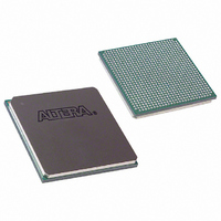
EP1S10F780I6N Altera, EP1S10F780I6N Datasheet - Page 368

EP1S10F780I6N
Manufacturer Part Number
EP1S10F780I6N
Description
IC STRATIX FPGA 10K LE 780-FBGA
Manufacturer
Altera
Series
Stratix®r
Datasheet
1.EP1S10F484I6N.pdf
(864 pages)
Specifications of EP1S10F780I6N
Number Of Logic Elements/cells
10570
Number Of Labs/clbs
1057
Total Ram Bits
920448
Number Of I /o
426
Voltage - Supply
1.425 V ~ 1.575 V
Mounting Type
Surface Mount
Operating Temperature
0°C ~ 85°C
Package / Case
780-FBGA
Lead Free Status / RoHS Status
Lead free / RoHS Compliant
Number Of Gates
-
Available stocks
Company
Part Number
Manufacturer
Quantity
Price
Company:
Part Number:
EP1S10F780I6N
Manufacturer:
ALTERA
Quantity:
3 000
- Current page: 368 of 864
- Download datasheet (11Mb)
Memory
Section II–2
Chapter
3
November 2003,
June 2006, v3.3
April 2004, v3.0
July 2005, v3.2
July 2003, v2.0
Date/Version
September
2004, v3.1
v2.1
●
●
●
●
●
●
●
●
●
●
●
●
●
●
●
●
●
●
●
●
●
Changed the name of the chapter from External Memory
Interfaces to External Memory Interfaces in Stratix &
Stratix GX Devices to reflect its shared status between
those device handbooks.
Added cross reference regarding frequency limits for 72
and 90
Updated mathematical symbols in
Updated
Moved Figure 8 to become Figure 1,
a DQS Signal is Center-Aligned in the IOE” on page
Updated
4, 5, and 6, are now Note 5, 6, and 7, respectively.
Updated
Updated
Updated Note on
Moved the
follow the Introduction section.
Moved
Chapter renamed
in Stratix & Stratix GX
Table
SRAM row updated.
Added
DQSn pins removed (page 3-5)
Deleted “QDR SRAM Interfacing” figure.
Replaced “t
Removed support for series and parallel on-chip
termination.
altddio_bidir function is used for DQS in versions before
Quartus II 3.0. (page 3-2)
Updated naming convention for DQS pins on page 3-9 to
match pin tables.
Clarified input clock to PLL must come from an external
input pin on page 3-12.
3–1: DDR SDRAM - side banks row added, ZBT
°
Tables 3–2
“Conclusion” on page 3–27
phase shift for DQS.
“DQS Phase-Shift Circuitry”
Table 3–1 on page
Table 3–2 on page
Table 3–3 on page
“External Memory Standards” on page 3–1
ZX
& t
XZ
page
Chapter 3, External Memory Interfaces
and 3–4.
Changes Made
Timing Diagram.”
Devices.
3–14.
3–10, updated Note 4. Note
3–10.
3–13.
Table
to end of chapter.
“Example of Where
section.
Stratix Device Handbook, Volume 2
3–3.
3–3.
to
Altera Corporation
Comments
Related parts for EP1S10F780I6N
Image
Part Number
Description
Manufacturer
Datasheet
Request
R

Part Number:
Description:
CYCLONE II STARTER KIT EP2C20N
Manufacturer:
Altera
Datasheet:

Part Number:
Description:
CPLD, EP610 Family, ECMOS Process, 300 Gates, 16 Macro Cells, 16 Reg., 16 User I/Os, 5V Supply, 35 Speed Grade, 24DIP
Manufacturer:
Altera Corporation
Datasheet:

Part Number:
Description:
CPLD, EP610 Family, ECMOS Process, 300 Gates, 16 Macro Cells, 16 Reg., 16 User I/Os, 5V Supply, 15 Speed Grade, 24DIP
Manufacturer:
Altera Corporation
Datasheet:

Part Number:
Description:
Manufacturer:
Altera Corporation
Datasheet:

Part Number:
Description:
CPLD, EP610 Family, ECMOS Process, 300 Gates, 16 Macro Cells, 16 Reg., 16 User I/Os, 5V Supply, 30 Speed Grade, 24DIP
Manufacturer:
Altera Corporation
Datasheet:

Part Number:
Description:
High-performance, low-power erasable programmable logic devices with 8 macrocells, 10ns
Manufacturer:
Altera Corporation
Datasheet:

Part Number:
Description:
High-performance, low-power erasable programmable logic devices with 8 macrocells, 7ns
Manufacturer:
Altera Corporation
Datasheet:

Part Number:
Description:
Classic EPLD
Manufacturer:
Altera Corporation
Datasheet:

Part Number:
Description:
High-performance, low-power erasable programmable logic devices with 8 macrocells, 10ns
Manufacturer:
Altera Corporation
Datasheet:

Part Number:
Description:
Manufacturer:
Altera Corporation
Datasheet:

Part Number:
Description:
Manufacturer:
Altera Corporation
Datasheet:

Part Number:
Description:
Manufacturer:
Altera Corporation
Datasheet:

Part Number:
Description:
CPLD, EP610 Family, ECMOS Process, 300 Gates, 16 Macro Cells, 16 Reg., 16 User I/Os, 5V Supply, 25 Speed Grade, 24DIP
Manufacturer:
Altera Corporation
Datasheet:


