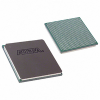
EP1S10F780I6N Altera, EP1S10F780I6N Datasheet - Page 755

EP1S10F780I6N
Manufacturer Part Number
EP1S10F780I6N
Description
IC STRATIX FPGA 10K LE 780-FBGA
Manufacturer
Altera
Series
Stratix®r
Datasheet
1.EP1S10F484I6N.pdf
(864 pages)
Specifications of EP1S10F780I6N
Number Of Logic Elements/cells
10570
Number Of Labs/clbs
1057
Total Ram Bits
920448
Number Of I /o
426
Voltage - Supply
1.425 V ~ 1.575 V
Mounting Type
Surface Mount
Operating Temperature
0°C ~ 85°C
Package / Case
780-FBGA
Lead Free Status / RoHS Status
Lead free / RoHS Compliant
Number Of Gates
-
Available stocks
Company
Part Number
Manufacturer
Quantity
Price
Company:
Part Number:
EP1S10F780I6N
Manufacturer:
ALTERA
Quantity:
3 000
- Current page: 755 of 864
- Download datasheet (11Mb)
Altera Corporation
July 2005
TDI
TDO
TMS
TCK
TRST
Table 11–11. JTAG Pin Descriptions
Pin
Test data input
Test data output
Test mode select
Test clock input
Test reset input
(optional)
Description
f
f
probes and capture functional data while a device is operating normally.
You can also use the JTAG circuitry to shift configuration data into the
device.
For more information on JTAG boundary-scan testing, see AN 39: IEEE
1149.1 (JTAG) Boundary-Scan Testing in Altera Devices.
To use the SignalTap
the JTAG pins of your Stratix device to a download cable header on your
PCB.
For more information on SignalTap II, see the Design Debugging Using
SignalTap II Embedded Logic Analyzer chapter in the Quartus II Handbook,
Volume 2.
A device operating in JTAG mode uses four required pins, TDI, TDO, TMS,
and TCK, and one optional pin, TRST. The four JTAG input pins (TDI,
TMS, TCK and TRST) have weak, internal pull-up resistors, whose values
range from 20 to 40 k . All other pins are tri-stated during JTAG
configuration. Do not begin JTAG configuration until all other
configuration is complete.
Serial input pin for instructions as well as test and programming data. Data is
The clock input to the BST circuitry. Some operations occur at the rising edge,
shifted in on the rising edge of
selection.
Serial data output pin for instructions as well as test and programming data. Data
is shifted out on the falling edge of
shifted out of the device. The high level output voltage is determined by VCCIO.
Input pin that provides the control signal to determine the transitions of the Test
Access Port
occur on the rising edge of
edge of
controls the input buffer selection.
while others occur at the falling edge. The
selection.
Active-low input to asynchronously reset the boundary-scan circuit. The
pin is optional according to IEEE Std. 1149.1. The
buffer selection.
TCK
(
.
TAP) controller state machine. Transitions within the state machine
TMS
is evaluated on the rising edge of
®
II embedded logic analyzer, you need to connect
TCK
Table 11–11
TCK
. Therefore,
TCK
. The
Function
Configuring Stratix & Stratix GX Devices
. The pin is tri-stated if data is not being
VCCSEL
shows each JTAG pin’s function.
VCCSEL
Stratix Device Handbook, Volume 2
TMS
must be set up before the rising
VCCSEL
pin controls the input buffer
pin controls the input buffer
TCK
. The
pin controls the input
VCCSEL
pin
TRST
11–37
Related parts for EP1S10F780I6N
Image
Part Number
Description
Manufacturer
Datasheet
Request
R

Part Number:
Description:
CYCLONE II STARTER KIT EP2C20N
Manufacturer:
Altera
Datasheet:

Part Number:
Description:
CPLD, EP610 Family, ECMOS Process, 300 Gates, 16 Macro Cells, 16 Reg., 16 User I/Os, 5V Supply, 35 Speed Grade, 24DIP
Manufacturer:
Altera Corporation
Datasheet:

Part Number:
Description:
CPLD, EP610 Family, ECMOS Process, 300 Gates, 16 Macro Cells, 16 Reg., 16 User I/Os, 5V Supply, 15 Speed Grade, 24DIP
Manufacturer:
Altera Corporation
Datasheet:

Part Number:
Description:
Manufacturer:
Altera Corporation
Datasheet:

Part Number:
Description:
CPLD, EP610 Family, ECMOS Process, 300 Gates, 16 Macro Cells, 16 Reg., 16 User I/Os, 5V Supply, 30 Speed Grade, 24DIP
Manufacturer:
Altera Corporation
Datasheet:

Part Number:
Description:
High-performance, low-power erasable programmable logic devices with 8 macrocells, 10ns
Manufacturer:
Altera Corporation
Datasheet:

Part Number:
Description:
High-performance, low-power erasable programmable logic devices with 8 macrocells, 7ns
Manufacturer:
Altera Corporation
Datasheet:

Part Number:
Description:
Classic EPLD
Manufacturer:
Altera Corporation
Datasheet:

Part Number:
Description:
High-performance, low-power erasable programmable logic devices with 8 macrocells, 10ns
Manufacturer:
Altera Corporation
Datasheet:

Part Number:
Description:
Manufacturer:
Altera Corporation
Datasheet:

Part Number:
Description:
Manufacturer:
Altera Corporation
Datasheet:

Part Number:
Description:
Manufacturer:
Altera Corporation
Datasheet:

Part Number:
Description:
CPLD, EP610 Family, ECMOS Process, 300 Gates, 16 Macro Cells, 16 Reg., 16 User I/Os, 5V Supply, 25 Speed Grade, 24DIP
Manufacturer:
Altera Corporation
Datasheet:


