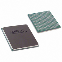
EP1S10F780I6N Altera, EP1S10F780I6N Datasheet - Page 407

EP1S10F780I6N
Manufacturer Part Number
EP1S10F780I6N
Description
IC STRATIX FPGA 10K LE 780-FBGA
Manufacturer
Altera
Series
Stratix®r
Datasheet
1.EP1S10F484I6N.pdf
(864 pages)
Specifications of EP1S10F780I6N
Number Of Logic Elements/cells
10570
Number Of Labs/clbs
1057
Total Ram Bits
920448
Number Of I /o
426
Voltage - Supply
1.425 V ~ 1.575 V
Mounting Type
Surface Mount
Operating Temperature
0°C ~ 85°C
Package / Case
780-FBGA
Lead Free Status / RoHS Status
Lead free / RoHS Compliant
Number Of Gates
-
Available stocks
Company
Part Number
Manufacturer
Quantity
Price
Company:
Part Number:
EP1S10F780I6N
Manufacturer:
ALTERA
Quantity:
3 000
- Current page: 407 of 864
- Download datasheet (11Mb)
Altera Corporation
June 2006
Notes to
(1)
(2)
(3)
(4)
(5)
ZBT SRAM
Table 3–2. External RAM Support in Stratix EP1S60 & EP1S80 (Part 2 of 2)
These maximum clock rates apply if the Stratix device uses DQS phase-shift circuitry to interface with DDR
SDRAM. DQS phase-shift circuitry is only available on the top and bottom I/O banks (I/O banks 3, 4, 7, and 8).
For more information on DDR SDRAM, see AN 342: Interfacing DDR SDRAM with Stratix & Stratix GX Devices.
DDR SDRAM is supported on the side banks (I/O banks 1, 2, 5, and 6) with no dedicated DQS phase-shift circuitry.
The read DQS signal is ignored in this mode.
For more information on QDR or QDRII SRAM, see AN 349: QDR SRAM Controller Reference Design for Stratix &
Stratix GX Devices.
For more information on ZBT SRAM, see AN 329: ZBT SRAM Controller Reference Design for Stratix and Stratix GX
Devices.
DDR Memory Type
Table
(5)
3–2:
f
Stratix and Stratix GX devices support the data strobe or read clock signal
(DQS) used in DDR SDRAM, and RLDRAM II devices. DQS signals are
associated with a group of data (DQ) pins.
Stratix and Stratix GX devices contain dedicated circuitry to shift the
incoming DQS signals by 0°, 72°, and 90°. The DQS phase-shift circuitry
uses a frequency reference to dynamically generate control signals for the
delay chains in each of the DQS pins, allowing it to compensate for
process, voltage, and temperature (PVT) variations. The dedicated
circuitry also creates consistent margins that meet your data sampling
window requirements.
Refer to the DC & Switching Characteristics chapter in volume 1 of the
Stratix Device Handbook for frequency limits regarding the 72 and 90°
phase shift for DQS.
In addition to the DQS dedicated phase-shift circuitry, every I/O element
(IOE) in Stratix and Stratix GX devices contains six registers and one latch
to achieve DDR operation. There is also a programmable delay chain in
the IOE that can help reduce contention when interfacing with ZBT
SRAM devices.
DDR Memory Interface Pins
Stratix and Stratix GX devices use data (DQ), data strobe (DQS), and clock
pins to interface with DDR SDRAM and RLDRAM II devices. This section
explains the pins used in the DDR SDRAM and RLDRAM II interfaces.
For QDR, QDRII, and ZBT SRAM interfaces, see the
Standards”
LVTTL
I/O Standard
section.
External Memory Interfaces in Stratix & Stratix GX Devices
-5 Speed Grade
200
Maximum Clock Rate (MHz)
Stratix Device Handbook, Volume 2
-6 Speed Grade -7 Speed Grade
200
“External Memory
167
3–11
Related parts for EP1S10F780I6N
Image
Part Number
Description
Manufacturer
Datasheet
Request
R

Part Number:
Description:
CYCLONE II STARTER KIT EP2C20N
Manufacturer:
Altera
Datasheet:

Part Number:
Description:
CPLD, EP610 Family, ECMOS Process, 300 Gates, 16 Macro Cells, 16 Reg., 16 User I/Os, 5V Supply, 35 Speed Grade, 24DIP
Manufacturer:
Altera Corporation
Datasheet:

Part Number:
Description:
CPLD, EP610 Family, ECMOS Process, 300 Gates, 16 Macro Cells, 16 Reg., 16 User I/Os, 5V Supply, 15 Speed Grade, 24DIP
Manufacturer:
Altera Corporation
Datasheet:

Part Number:
Description:
Manufacturer:
Altera Corporation
Datasheet:

Part Number:
Description:
CPLD, EP610 Family, ECMOS Process, 300 Gates, 16 Macro Cells, 16 Reg., 16 User I/Os, 5V Supply, 30 Speed Grade, 24DIP
Manufacturer:
Altera Corporation
Datasheet:

Part Number:
Description:
High-performance, low-power erasable programmable logic devices with 8 macrocells, 10ns
Manufacturer:
Altera Corporation
Datasheet:

Part Number:
Description:
High-performance, low-power erasable programmable logic devices with 8 macrocells, 7ns
Manufacturer:
Altera Corporation
Datasheet:

Part Number:
Description:
Classic EPLD
Manufacturer:
Altera Corporation
Datasheet:

Part Number:
Description:
High-performance, low-power erasable programmable logic devices with 8 macrocells, 10ns
Manufacturer:
Altera Corporation
Datasheet:

Part Number:
Description:
Manufacturer:
Altera Corporation
Datasheet:

Part Number:
Description:
Manufacturer:
Altera Corporation
Datasheet:

Part Number:
Description:
Manufacturer:
Altera Corporation
Datasheet:

Part Number:
Description:
CPLD, EP610 Family, ECMOS Process, 300 Gates, 16 Macro Cells, 16 Reg., 16 User I/Os, 5V Supply, 25 Speed Grade, 24DIP
Manufacturer:
Altera Corporation
Datasheet:


