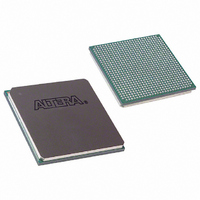
EP1S10F780I6N Altera, EP1S10F780I6N Datasheet - Page 415

EP1S10F780I6N
Manufacturer Part Number
EP1S10F780I6N
Description
IC STRATIX FPGA 10K LE 780-FBGA
Manufacturer
Altera
Series
Stratix®r
Datasheet
1.EP1S10F484I6N.pdf
(864 pages)
Specifications of EP1S10F780I6N
Number Of Logic Elements/cells
10570
Number Of Labs/clbs
1057
Total Ram Bits
920448
Number Of I /o
426
Voltage - Supply
1.425 V ~ 1.575 V
Mounting Type
Surface Mount
Operating Temperature
0°C ~ 85°C
Package / Case
780-FBGA
Lead Free Status / RoHS Status
Lead free / RoHS Compliant
Number Of Gates
-
Available stocks
Company
Part Number
Manufacturer
Quantity
Price
Company:
Part Number:
EP1S10F780I6N
Manufacturer:
ALTERA
Quantity:
3 000
- Current page: 415 of 864
- Download datasheet (11Mb)
Altera Corporation
June 2006
f
Figure 3–9. Simplified Diagram of the DQS Phase-Shift Circuitry
The input reference clock goes into the DLL to a chain of delay elements.
The phase comparator compares the signal coming out of the end of the
delay element chain to the input reference clock. The phase comparator
then issues the upndn signal to the up/down counter. This signal
increments or decrements a six-bit delay setting (control signals to DQS
pins) that increases or decreases the delay through the delay element
chain to bring the input reference clock and the signals coming out of the
delay element chain in phase.
The shifted DQS signal then goes to the DQS bus to clock the IOE input
registers of the DQ pins. It cannot go into the logic array for other
purposes.
For external memory interfaces that use a bidirectional read strobe like
DDR SDRAM, the DQS signal is low before going to or coming from a
high-impedance state (see
is low just after a high-impedance state is called the preamble and the
state where DQS is low just before it returns to high-impedance state is
called the postamble. There are preamble and postamble specifications
for both read and write operations in DDR SDRAM. To ensure data is not
lost when there is noise on the DQS line at the end of a read postamble
time, you need to add soft postamble circuitry to disable the clocks at the
DQ IOE registers.
For more information, the DQS Postamble soft logic is described in
AN 342: Interfacing DDR SDRAM with Stratix & Stratix GX Devices. The
Altera DDR SDRAM controller MegaCore
open-source code.
Reference
Clock
Input
External Memory Interfaces in Stratix & Stratix GX Devices
Comparator
Phase
Figure 3–1 on page
Delay Chains
Stratix Device Handbook, Volume 2
Up/Down
Counter
®
generates this logic as
3–3). The state where DQS
6
Control Signals
to DQS Pins
3–19
Related parts for EP1S10F780I6N
Image
Part Number
Description
Manufacturer
Datasheet
Request
R

Part Number:
Description:
CYCLONE II STARTER KIT EP2C20N
Manufacturer:
Altera
Datasheet:

Part Number:
Description:
CPLD, EP610 Family, ECMOS Process, 300 Gates, 16 Macro Cells, 16 Reg., 16 User I/Os, 5V Supply, 35 Speed Grade, 24DIP
Manufacturer:
Altera Corporation
Datasheet:

Part Number:
Description:
CPLD, EP610 Family, ECMOS Process, 300 Gates, 16 Macro Cells, 16 Reg., 16 User I/Os, 5V Supply, 15 Speed Grade, 24DIP
Manufacturer:
Altera Corporation
Datasheet:

Part Number:
Description:
Manufacturer:
Altera Corporation
Datasheet:

Part Number:
Description:
CPLD, EP610 Family, ECMOS Process, 300 Gates, 16 Macro Cells, 16 Reg., 16 User I/Os, 5V Supply, 30 Speed Grade, 24DIP
Manufacturer:
Altera Corporation
Datasheet:

Part Number:
Description:
High-performance, low-power erasable programmable logic devices with 8 macrocells, 10ns
Manufacturer:
Altera Corporation
Datasheet:

Part Number:
Description:
High-performance, low-power erasable programmable logic devices with 8 macrocells, 7ns
Manufacturer:
Altera Corporation
Datasheet:

Part Number:
Description:
Classic EPLD
Manufacturer:
Altera Corporation
Datasheet:

Part Number:
Description:
High-performance, low-power erasable programmable logic devices with 8 macrocells, 10ns
Manufacturer:
Altera Corporation
Datasheet:

Part Number:
Description:
Manufacturer:
Altera Corporation
Datasheet:

Part Number:
Description:
Manufacturer:
Altera Corporation
Datasheet:

Part Number:
Description:
Manufacturer:
Altera Corporation
Datasheet:

Part Number:
Description:
CPLD, EP610 Family, ECMOS Process, 300 Gates, 16 Macro Cells, 16 Reg., 16 User I/Os, 5V Supply, 25 Speed Grade, 24DIP
Manufacturer:
Altera Corporation
Datasheet:


