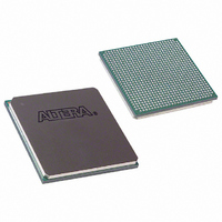
EP1S10F780I6N Altera, EP1S10F780I6N Datasheet - Page 537

EP1S10F780I6N
Manufacturer Part Number
EP1S10F780I6N
Description
IC STRATIX FPGA 10K LE 780-FBGA
Manufacturer
Altera
Series
Stratix®r
Datasheet
1.EP1S10F484I6N.pdf
(864 pages)
Specifications of EP1S10F780I6N
Number Of Logic Elements/cells
10570
Number Of Labs/clbs
1057
Total Ram Bits
920448
Number Of I /o
426
Voltage - Supply
1.425 V ~ 1.575 V
Mounting Type
Surface Mount
Operating Temperature
0°C ~ 85°C
Package / Case
780-FBGA
Lead Free Status / RoHS Status
Lead free / RoHS Compliant
Number Of Gates
-
Available stocks
Company
Part Number
Manufacturer
Quantity
Price
Company:
Part Number:
EP1S10F780I6N
Manufacturer:
ALTERA
Quantity:
3 000
- Current page: 537 of 864
- Download datasheet (11Mb)
Altera Corporation
July 2005
Notes to
(1)
(2)
(3)
tx_in[Deserialization_factor *
number_of_channels - 1..0]
tx_inclock
tx_pll_enable
tx_out[number_of_channels - 1..0]
tx_outclock
tx_coreclock
tx_locked
Table 5–16. LVDS Transmitter Ports
This is an optional port.
Only one tx_pll_enable pin is necessary to enable all the PLLs in the device.
This is a non-differential pin.
Table
5–16:
Port Name
LVDS Transmitter Module
The Quartus II software calculates the inclock boost (W) factor for the
LVDS transmitter based on input data rate, input clock frequency, and
the deserialization factor. In addition to setting the data and clock
alignment, you can also set the outclock divide factor (B) for the
transmitter output clock and add the pll_enable, tx_locked, and
tx_coreclock ports.
ports in the LVDS transmitter block.
You can also use the altlvds MegaWizard Plug-In Manager to create an
LVDS transmitter block. The following sections explain the parameters
available in the Plug-In Manager when creating an LVDS transmitter
block.
Page 3 of the altlvds_tx MegaWizard Plug-In Manager
This section describes the parameters found on page 3 of the
altlvds_tx MegaWizard Plug-In Manager (see
Input
Input
Input
Output
Output
Output
Output
Direction
High-Speed Differential I/O Interfaces in Stratix Devices
Table 5–16
Input data
Reference input clock
Fast PLL enable
Serialized LVDS data
signal
External reference clock
Internal reference clock
Fast PLL locked pin
explains the function of the available
Function
Stratix Device Handbook, Volume 2
Figure
Pin or output clock
Pin
Pin, logic array, or
Logic array
from a PLL
Pin (1), (2),
Pin
input clock to a fast
PLL
Pin or logic array (1),
(2),
Source/Output port
(3)
(1)
Destination
5–42).
Input port
(3)
5–65
Related parts for EP1S10F780I6N
Image
Part Number
Description
Manufacturer
Datasheet
Request
R

Part Number:
Description:
CYCLONE II STARTER KIT EP2C20N
Manufacturer:
Altera
Datasheet:

Part Number:
Description:
CPLD, EP610 Family, ECMOS Process, 300 Gates, 16 Macro Cells, 16 Reg., 16 User I/Os, 5V Supply, 35 Speed Grade, 24DIP
Manufacturer:
Altera Corporation
Datasheet:

Part Number:
Description:
CPLD, EP610 Family, ECMOS Process, 300 Gates, 16 Macro Cells, 16 Reg., 16 User I/Os, 5V Supply, 15 Speed Grade, 24DIP
Manufacturer:
Altera Corporation
Datasheet:

Part Number:
Description:
Manufacturer:
Altera Corporation
Datasheet:

Part Number:
Description:
CPLD, EP610 Family, ECMOS Process, 300 Gates, 16 Macro Cells, 16 Reg., 16 User I/Os, 5V Supply, 30 Speed Grade, 24DIP
Manufacturer:
Altera Corporation
Datasheet:

Part Number:
Description:
High-performance, low-power erasable programmable logic devices with 8 macrocells, 10ns
Manufacturer:
Altera Corporation
Datasheet:

Part Number:
Description:
High-performance, low-power erasable programmable logic devices with 8 macrocells, 7ns
Manufacturer:
Altera Corporation
Datasheet:

Part Number:
Description:
Classic EPLD
Manufacturer:
Altera Corporation
Datasheet:

Part Number:
Description:
High-performance, low-power erasable programmable logic devices with 8 macrocells, 10ns
Manufacturer:
Altera Corporation
Datasheet:

Part Number:
Description:
Manufacturer:
Altera Corporation
Datasheet:

Part Number:
Description:
Manufacturer:
Altera Corporation
Datasheet:

Part Number:
Description:
Manufacturer:
Altera Corporation
Datasheet:

Part Number:
Description:
CPLD, EP610 Family, ECMOS Process, 300 Gates, 16 Macro Cells, 16 Reg., 16 User I/Os, 5V Supply, 25 Speed Grade, 24DIP
Manufacturer:
Altera Corporation
Datasheet:


