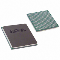
EP1S10F780I6N Altera, EP1S10F780I6N Datasheet - Page 709

EP1S10F780I6N
Manufacturer Part Number
EP1S10F780I6N
Description
IC STRATIX FPGA 10K LE 780-FBGA
Manufacturer
Altera
Series
Stratix®r
Datasheet
1.EP1S10F484I6N.pdf
(864 pages)
Specifications of EP1S10F780I6N
Number Of Logic Elements/cells
10570
Number Of Labs/clbs
1057
Total Ram Bits
920448
Number Of I /o
426
Voltage - Supply
1.425 V ~ 1.575 V
Mounting Type
Surface Mount
Operating Temperature
0°C ~ 85°C
Package / Case
780-FBGA
Lead Free Status / RoHS Status
Lead free / RoHS Compliant
Number Of Gates
-
Available stocks
Company
Part Number
Manufacturer
Quantity
Price
Company:
Part Number:
EP1S10F780I6N
Manufacturer:
ALTERA
Quantity:
3 000
- Current page: 709 of 864
- Download datasheet (11Mb)
I/O Structure
Altera Corporation
July 2005
f
■
Therefore, you can enter different project clock settings corresponding to
new PLL settings and accelerate timing analysis by eliminating a full
compilation cycle.
For more information about using Stratix and Stratix GX PLLs, see the
General-Purpose PLLs in Stratix & Stratix GX Devices chapter.
The Stratix and Stratix GX I/O element (IOE) architecture is similar to the
APEX II architecture, with a total of six registers and a latch in each IOE.
The registers are organized in three sets: two output registers to drive a
single or double-data rate (DDR) output path, two input registers and a
latch to support a single or DDR input path, and two output enable
registers to enhance clock-to-output enable timing or for DDR SDRAM
interfacing. A new synchronous reset signal is available to each of the
three sets of registers for preset or clear, or neither. In addition to the
advanced IOE architecture, the Stratix and Stratix GX IOE features
dedicated circuitry for external RAM interfacing, new I/O standards,
differential on-chip termination, and high-speed differential I/O
standard support.
External RAM Interfacing
The advanced Stratix and Stratix GX IOE architecture includes dedicated
circuitry to interface with external RAM. This circuitry provides
enhanced support for external high-speed memory devices such as DDR
SDRAM and FCRAM. The DDR SDRAM interface uses a bidirectional
signal, DQS, to clock data, DQ, at both the transmitting and receiving
device. Stratix and Stratix GX devices transmit the DQS signal with the DQ
data signals to minimize clock to data skew.
Stratix and Stratix GX devices include groups of programmable DQS and
DQ pins, in the top and bottom I/O banks of the device. Each group
consists of a DQS pin that supports a fixed number of DQ pins. The number
of DQ pins depends on the DQ bus mode. When using the external RAM
interfacing circuitry, the DQS pin drives a dedicated clock network that
feeds the DQ pins residing in that bank. The Stratix and Stratix GX IOE has
programmable delay chains that can phase shift the DQS signal by 90° or
72° to ensure data is sampled at the appropriate point in time. Therefore,
the Stratix and Stratix GX devices make full use of the IOEs, and remove
the need to build the input data path in the logic array. You can make
these I/O assignments in the Quartus II Assignment Organizer.
A Default Required f
settings. Only individual clock settings override the PLL clock
settings.
Transitioning APEX Designs to Stratix & Stratix GX Devices
MAX
setting does not override the PLL clock
Stratix Device Handbook, Volume 2
10–25
Related parts for EP1S10F780I6N
Image
Part Number
Description
Manufacturer
Datasheet
Request
R

Part Number:
Description:
CYCLONE II STARTER KIT EP2C20N
Manufacturer:
Altera
Datasheet:

Part Number:
Description:
CPLD, EP610 Family, ECMOS Process, 300 Gates, 16 Macro Cells, 16 Reg., 16 User I/Os, 5V Supply, 35 Speed Grade, 24DIP
Manufacturer:
Altera Corporation
Datasheet:

Part Number:
Description:
CPLD, EP610 Family, ECMOS Process, 300 Gates, 16 Macro Cells, 16 Reg., 16 User I/Os, 5V Supply, 15 Speed Grade, 24DIP
Manufacturer:
Altera Corporation
Datasheet:

Part Number:
Description:
Manufacturer:
Altera Corporation
Datasheet:

Part Number:
Description:
CPLD, EP610 Family, ECMOS Process, 300 Gates, 16 Macro Cells, 16 Reg., 16 User I/Os, 5V Supply, 30 Speed Grade, 24DIP
Manufacturer:
Altera Corporation
Datasheet:

Part Number:
Description:
High-performance, low-power erasable programmable logic devices with 8 macrocells, 10ns
Manufacturer:
Altera Corporation
Datasheet:

Part Number:
Description:
High-performance, low-power erasable programmable logic devices with 8 macrocells, 7ns
Manufacturer:
Altera Corporation
Datasheet:

Part Number:
Description:
Classic EPLD
Manufacturer:
Altera Corporation
Datasheet:

Part Number:
Description:
High-performance, low-power erasable programmable logic devices with 8 macrocells, 10ns
Manufacturer:
Altera Corporation
Datasheet:

Part Number:
Description:
Manufacturer:
Altera Corporation
Datasheet:

Part Number:
Description:
Manufacturer:
Altera Corporation
Datasheet:

Part Number:
Description:
Manufacturer:
Altera Corporation
Datasheet:

Part Number:
Description:
CPLD, EP610 Family, ECMOS Process, 300 Gates, 16 Macro Cells, 16 Reg., 16 User I/Os, 5V Supply, 25 Speed Grade, 24DIP
Manufacturer:
Altera Corporation
Datasheet:


