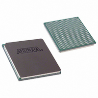
EP1S10F780I6N Altera, EP1S10F780I6N Datasheet - Page 539

EP1S10F780I6N
Manufacturer Part Number
EP1S10F780I6N
Description
IC STRATIX FPGA 10K LE 780-FBGA
Manufacturer
Altera
Series
Stratix®r
Datasheet
1.EP1S10F484I6N.pdf
(864 pages)
Specifications of EP1S10F780I6N
Number Of Logic Elements/cells
10570
Number Of Labs/clbs
1057
Total Ram Bits
920448
Number Of I /o
426
Voltage - Supply
1.425 V ~ 1.575 V
Mounting Type
Surface Mount
Operating Temperature
0°C ~ 85°C
Package / Case
780-FBGA
Lead Free Status / RoHS Status
Lead free / RoHS Compliant
Number Of Gates
-
Available stocks
Company
Part Number
Manufacturer
Quantity
Price
Company:
Part Number:
EP1S10F780I6N
Manufacturer:
ALTERA
Quantity:
3 000
- Current page: 539 of 864
- Download datasheet (11Mb)
Altera Corporation
July 2005
deserialization factor. The total width of the tx_in port of the transmitter
is equal to the number of channels multiplied by the deserialization
factor.
Outclock Divide Factor
The What is the Output data rate? parameter specifies the ratio of the
tx_outclock frequency compared to the data rate. The default value for
this parameter is the value of the deserialization factor parameter. The
tx_outclock frequency is equal to [W/B] x input clock frequency.
There is also an optional tx_coreclock port which has the same
frequency as the [W/J]
The outclock divide factor is useful for applications that do not require
the data rate to be the same as the clock frequency. For example,
HyperTransport technology uses a half-clock data rate scheme where the
clock frequency is half the data rate.
outclock divide factor for a given deserialization factor.
Output Data Rate
The What is the Output data rate parameter specifies the data rate out of
the fast PLL and determines the input clock boost/multiplication factor
needed for the transmitter. This parameter must be larger than the input
clock frequency and has a maximum rate of 840 Mbps for Stratix devices.
The input clock boost factor (W) is the output data rate divided by the
input clock frequency. The Stratix SERDES circuitry supports input clock
boost factors of 4, 7, 8, or 10. The maximum output data rate is 840 Mbps,
while the clock has a maximum output of 500 MHz.
Data Alignment with Clock
Use the What is the alignment of data with respect to tx_inclock?
parameter and the What is the alignment of tx_outclock? to align the
input and output data, respectively, with the clock. For most applications,
the data is edge-aligned with the clock. However, there are applications
where the data must be center-aligned with respect to the clock. With
Note to
(1)
Table 5–17. Deserialization Factor (J) vs. Outclock Divide Factor (B)
The clock does not have a 50% duty cycle when b=7 in x7 mode.
Deserialization Factor (J)
Table
5–17:
10
4
7
8
High-Speed Differential I/O Interfaces in Stratix Devices
×
input frequency.
Table 5–17
Stratix Device Handbook, Volume 2
Outclock Divide Factor (B)
shows the supported
1, 2, 4, 8
1, 2, 10
1, 2, 4
1,
7(1)
5–67
Related parts for EP1S10F780I6N
Image
Part Number
Description
Manufacturer
Datasheet
Request
R

Part Number:
Description:
CYCLONE II STARTER KIT EP2C20N
Manufacturer:
Altera
Datasheet:

Part Number:
Description:
CPLD, EP610 Family, ECMOS Process, 300 Gates, 16 Macro Cells, 16 Reg., 16 User I/Os, 5V Supply, 35 Speed Grade, 24DIP
Manufacturer:
Altera Corporation
Datasheet:

Part Number:
Description:
CPLD, EP610 Family, ECMOS Process, 300 Gates, 16 Macro Cells, 16 Reg., 16 User I/Os, 5V Supply, 15 Speed Grade, 24DIP
Manufacturer:
Altera Corporation
Datasheet:

Part Number:
Description:
Manufacturer:
Altera Corporation
Datasheet:

Part Number:
Description:
CPLD, EP610 Family, ECMOS Process, 300 Gates, 16 Macro Cells, 16 Reg., 16 User I/Os, 5V Supply, 30 Speed Grade, 24DIP
Manufacturer:
Altera Corporation
Datasheet:

Part Number:
Description:
High-performance, low-power erasable programmable logic devices with 8 macrocells, 10ns
Manufacturer:
Altera Corporation
Datasheet:

Part Number:
Description:
High-performance, low-power erasable programmable logic devices with 8 macrocells, 7ns
Manufacturer:
Altera Corporation
Datasheet:

Part Number:
Description:
Classic EPLD
Manufacturer:
Altera Corporation
Datasheet:

Part Number:
Description:
High-performance, low-power erasable programmable logic devices with 8 macrocells, 10ns
Manufacturer:
Altera Corporation
Datasheet:

Part Number:
Description:
Manufacturer:
Altera Corporation
Datasheet:

Part Number:
Description:
Manufacturer:
Altera Corporation
Datasheet:

Part Number:
Description:
Manufacturer:
Altera Corporation
Datasheet:

Part Number:
Description:
CPLD, EP610 Family, ECMOS Process, 300 Gates, 16 Macro Cells, 16 Reg., 16 User I/Os, 5V Supply, 25 Speed Grade, 24DIP
Manufacturer:
Altera Corporation
Datasheet:


