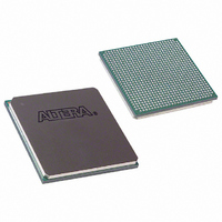
EP1S10F780I6N Altera, EP1S10F780I6N Datasheet - Page 400

EP1S10F780I6N
Manufacturer Part Number
EP1S10F780I6N
Description
IC STRATIX FPGA 10K LE 780-FBGA
Manufacturer
Altera
Series
Stratix®r
Datasheet
1.EP1S10F484I6N.pdf
(864 pages)
Specifications of EP1S10F780I6N
Number Of Logic Elements/cells
10570
Number Of Labs/clbs
1057
Total Ram Bits
920448
Number Of I /o
426
Voltage - Supply
1.425 V ~ 1.575 V
Mounting Type
Surface Mount
Operating Temperature
0°C ~ 85°C
Package / Case
780-FBGA
Lead Free Status / RoHS Status
Lead free / RoHS Compliant
Number Of Gates
-
Available stocks
Company
Part Number
Manufacturer
Quantity
Price
Company:
Part Number:
EP1S10F780I6N
Manufacturer:
ALTERA
Quantity:
3 000
- Current page: 400 of 864
- Download datasheet (11Mb)
External Memory Standards
Figure 3–3. DDR SDRAM Interfacing
3–4
Stratix Device Handbook, Volume 2
PLL
OE
− 90˚
Registers
f
f
DDR
OE
User logic/
GND
Figure 3–3
dedicated circuitry to the logic array. When the DQS pin acts as an input
strobe, the dedicated circuitry shifts the incoming DQS pin by either 72°
or 90° and clocks the DDR input registers. Because of the DDR input
registers architecture in Stratix and Stratix GX devices, the shifted DQS
signal must be inverted. The DDR registers outputs are sent to two LE
registers to be synchronized with the system clock.
Refer to the DC & Switching Characteristics chapter in volume 1 of the
Stratix Device Handbook for frequency limits regarding the 72 and 90°
phase shift for DQS.
For more information on DDR SDRAM specifications, see JEDEC
standard publications JESD79C from www.jedec.org, or see
AN 342: Interfacing DDR SDRAM with Stratix & Stratix GX Devices.
RLDRAM II
RLDRAM II provides fast random access as well as high bandwidth and
high density, making this memory technology ideal for high-speed
network and communication data storage applications. The fast random
access speeds in RLDRAM II devices make them a viable alternative to
SRAM devices at a lower cost. Additionally, RLDRAM II devices have
minimal latency to support designs that require fast response times.
2
Registers
Output
DDR
DQS
shows DDR SDRAM interfacing from the I/O through the
Δ t
Compensated
Delay Shift
OE
DQS Bus
Registers
DDR
OE
Resynchronizing
Global Clock
2
Registers
Output
DDR
DQ
Adjacent LAB LEs
Registers
Register
Register
DDR
Input
LE
LE
Altera Corporation
2
I/O Elements &
Periphery
June 2006
Related parts for EP1S10F780I6N
Image
Part Number
Description
Manufacturer
Datasheet
Request
R

Part Number:
Description:
CYCLONE II STARTER KIT EP2C20N
Manufacturer:
Altera
Datasheet:

Part Number:
Description:
CPLD, EP610 Family, ECMOS Process, 300 Gates, 16 Macro Cells, 16 Reg., 16 User I/Os, 5V Supply, 35 Speed Grade, 24DIP
Manufacturer:
Altera Corporation
Datasheet:

Part Number:
Description:
CPLD, EP610 Family, ECMOS Process, 300 Gates, 16 Macro Cells, 16 Reg., 16 User I/Os, 5V Supply, 15 Speed Grade, 24DIP
Manufacturer:
Altera Corporation
Datasheet:

Part Number:
Description:
Manufacturer:
Altera Corporation
Datasheet:

Part Number:
Description:
CPLD, EP610 Family, ECMOS Process, 300 Gates, 16 Macro Cells, 16 Reg., 16 User I/Os, 5V Supply, 30 Speed Grade, 24DIP
Manufacturer:
Altera Corporation
Datasheet:

Part Number:
Description:
High-performance, low-power erasable programmable logic devices with 8 macrocells, 10ns
Manufacturer:
Altera Corporation
Datasheet:

Part Number:
Description:
High-performance, low-power erasable programmable logic devices with 8 macrocells, 7ns
Manufacturer:
Altera Corporation
Datasheet:

Part Number:
Description:
Classic EPLD
Manufacturer:
Altera Corporation
Datasheet:

Part Number:
Description:
High-performance, low-power erasable programmable logic devices with 8 macrocells, 10ns
Manufacturer:
Altera Corporation
Datasheet:

Part Number:
Description:
Manufacturer:
Altera Corporation
Datasheet:

Part Number:
Description:
Manufacturer:
Altera Corporation
Datasheet:

Part Number:
Description:
Manufacturer:
Altera Corporation
Datasheet:

Part Number:
Description:
CPLD, EP610 Family, ECMOS Process, 300 Gates, 16 Macro Cells, 16 Reg., 16 User I/Os, 5V Supply, 25 Speed Grade, 24DIP
Manufacturer:
Altera Corporation
Datasheet:


