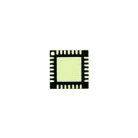
C8051F411-GMR Silicon Laboratories Inc, C8051F411-GMR Datasheet - Page 66

C8051F411-GMR
Manufacturer Part Number
C8051F411-GMR
Description
Microcontrollers (MCU) 50 MIPS 32KB 12ADC RTCLOCK 28 PIN MCU
Manufacturer
Silicon Laboratories Inc
Datasheet
1.C8051F410DK.pdf
(270 pages)
Specifications of C8051F411-GMR
Processor Series
C8051F4x
Core
8051
Data Bus Width
8 bit
Program Memory Type
Flash
Program Memory Size
32 KB
Data Ram Size
2.25 KB
Interface Type
I2C, SMBus, SPI, UART
Maximum Clock Frequency
50 MHz
Number Of Programmable I/os
20
Number Of Timers
4
Maximum Operating Temperature
+ 85 C
Mounting Style
SMD/SMT
Package / Case
QFN
3rd Party Development Tools
PK51, CA51, A51, ULINK2
Development Tools By Supplier
C8051F410DK
Minimum Operating Temperature
- 40 C
On-chip Adc
12 bit, 20 Channel
On-chip Dac
12 bit, 2 Channel
Package
28QFN EP
Device Core
8051
Family Name
C8051F41x
Maximum Speed
50 MHz
Ram Size
2.25 KB
Operating Supply Voltage
1.8|2.5|3.3|5 V
Operating Temperature
-40 to 85 °C
Lead Free Status / Rohs Status
Details
Available stocks
Company
Part Number
Manufacturer
Quantity
Price
Company:
Part Number:
C8051F411-GMR
Manufacturer:
SiliconL
Quantity:
3 000
Part Number:
C8051F411-GMR
Manufacturer:
SILICON LABS/芯科
Quantity:
20 000
- Current page: 66 of 270
- Download datasheet (2Mb)
C8051F410/1/2/3
5.4.1. Window Detector In Single-Ended Mode
Figure 5.7
ADC0LTH:ADC0LTL = 0x0200 (512d) and ADC0GTH:ADC0GTL = 0x0100 (256d). The input voltage can
range from ‘0’ to V
value. The repeat count is set to one. In the left example, an AD0WINT interrupt will be generated if the
ADC0 conversion word (ADC0H:ADC0L) is within the range defined by ADC0GTH:ADC0GTL and
ADC0LTH:ADC0LTL (if 0x0100 < ADC0H:ADC0L < 0x0200). In the right example, and AD0WINT interrupt
will be generated if the ADC0 conversion word is outside of the range defined by the ADC0GT and
ADC0LT registers (if ADC0H:ADC0L < 0x0100 or ADC0H:ADC0L > 0x0200). Figure 5.8 shows an exam-
ple using left-justified data with the same comparison values.
66
Figure 5.7. ADC Window Compare Example: Right-Justified Single-Ended Data
VREF x (4095/4096)
VREF x (4095/4096)
VREF x (512/4096)
VREF x (256/4096)
Figure 5.8. ADC Window Compare Example: Left-Justified Single-Ended Data
VREF x (512/4096)
VREF x (256/4096)
Input Voltage
(Px.x - GND)
Input Voltage
(Px.x - GND)
0
0
shows
ADC0H:ADC0L
ADC0H:ADC0L
REF
0x0FFF
0x01FF
0x00FF
0xFFF0
0x1FF0
0x0FF0
0x0201
0x0200
0x0101
0x0100
0x0000
0x2010
0x2000
0x1010
0x1000
0x0000
x (4095/4096) with respect to GND, and is represented by a 12-bit unsigned integer
two
example
ADC0GTH:ADC0GTL
ADC0LTH:ADC0LTL
ADC0GTH:ADC0GTL
ADC0LTH:ADC0LTL
not affected
not affected
AD0WINT
AD0WINT
not affected
not affected
AD0WINT
AD0WINT
AD0WINT=1
window
AD0WINT=1
Rev. 1.1
VREF x (512/4096)
VREF x (256/4096)
comparisons
VREF x (4095/4096)
VREF x (512/4096)
VREF x (256/4096)
VREF x (4095/
Input Voltage
(Px.x - GND)
Input Voltage
(Px.x - GND)
4096)
0
0
ADC0H:ADC0L
ADC0H:ADC0L
0x0FFF
0x0201
0x0200
0x01FF
0x0101
0x0100
0x00FF
0x0000
for
0xFFF0
0x1FF0
0x0FF0
0x2010
0x2000
0x1010
0x1000
0x0000
right-justified
ADC0GTH:ADC0GTL
ADC0LTH:ADC0LTL
ADC0GTH:ADC0GTL
ADC0LTH:ADC0LTL
not affected
AD0WINT
not affected
AD0WINT
AD0WINT=1
AD0WINT=1
data
AD0WINT=1
AD0WINT=1
with
Related parts for C8051F411-GMR
Image
Part Number
Description
Manufacturer
Datasheet
Request
R
Part Number:
Description:
SMD/C°/SINGLE-ENDED OUTPUT SILICON OSCILLATOR
Manufacturer:
Silicon Laboratories Inc
Part Number:
Description:
Manufacturer:
Silicon Laboratories Inc
Datasheet:
Part Number:
Description:
N/A N/A/SI4010 AES KEYFOB DEMO WITH LCD RX
Manufacturer:
Silicon Laboratories Inc
Datasheet:
Part Number:
Description:
N/A N/A/SI4010 SIMPLIFIED KEY FOB DEMO WITH LED RX
Manufacturer:
Silicon Laboratories Inc
Datasheet:
Part Number:
Description:
N/A/-40 TO 85 OC/EZLINK MODULE; F930/4432 HIGH BAND (REV E/B1)
Manufacturer:
Silicon Laboratories Inc
Part Number:
Description:
EZLink Module; F930/4432 Low Band (rev e/B1)
Manufacturer:
Silicon Laboratories Inc
Part Number:
Description:
I°/4460 10 DBM RADIO TEST CARD 434 MHZ
Manufacturer:
Silicon Laboratories Inc
Part Number:
Description:
I°/4461 14 DBM RADIO TEST CARD 868 MHZ
Manufacturer:
Silicon Laboratories Inc
Part Number:
Description:
I°/4463 20 DBM RFSWITCH RADIO TEST CARD 460 MHZ
Manufacturer:
Silicon Laboratories Inc
Part Number:
Description:
I°/4463 20 DBM RADIO TEST CARD 868 MHZ
Manufacturer:
Silicon Laboratories Inc
Part Number:
Description:
I°/4463 27 DBM RADIO TEST CARD 868 MHZ
Manufacturer:
Silicon Laboratories Inc
Part Number:
Description:
I°/4463 SKYWORKS 30 DBM RADIO TEST CARD 915 MHZ
Manufacturer:
Silicon Laboratories Inc
Part Number:
Description:
N/A N/A/-40 TO 85 OC/4463 RFMD 30 DBM RADIO TEST CARD 915 MHZ
Manufacturer:
Silicon Laboratories Inc
Part Number:
Description:
I°/4463 20 DBM RADIO TEST CARD 169 MHZ
Manufacturer:
Silicon Laboratories Inc


