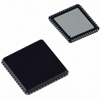
AD9995KCP Analog Devices Inc, AD9995KCP Datasheet - Page 10

AD9995KCP
Manufacturer Part Number
AD9995KCP
Description
IC CCD SIGNAL PROCESSOR 56-LFCSP
Manufacturer
Analog Devices Inc
Type
CCD Signal Processor, 12-Bitr
Datasheet
1.AD9995KCPZRL.pdf
(60 pages)
Specifications of AD9995KCP
Rohs Status
RoHS non-compliant
Input Type
Logic
Output Type
Logic
Interface
3-Wire Serial
Current - Supply
30mA
Mounting Type
Surface Mount
Package / Case
56-LFCSP
Analog Front End Type
CCD
Analog Front End Category
Video
Interface Type
Serial (3-Wire)
Input Voltage Range
0.5V
Operating Supply Voltage (min)
2.7V
Operating Supply Voltage (typ)
3V
Operating Supply Voltage (max)
3.6V
Resolution
12b
Number Of Adc's
1
Power Supply Type
Analog/Digital
Operating Temp Range
-20C to 85C
Operating Temperature Classification
Commercial
Mounting
Surface Mount
Pin Count
56
Package Type
LFCSP EP
Number Of Channels
1
Lead Free Status / RoHS Status
Not Compliant
Available stocks
Company
Part Number
Manufacturer
Quantity
Price
Company:
Part Number:
AD9995KCP
Manufacturer:
ADI
Quantity:
148
Company:
Part Number:
AD9995KCPZ
Manufacturer:
ADI
Quantity:
24
Company:
Part Number:
AD9995KCPZRL7
Manufacturer:
SANYO
Quantity:
1 170
PRECISION TIMING HIGH SPEED TIMING GENERATION
The AD9995 generates high speed timing signals using the
flexible Precision Timing core. This core is the foundation for
generating the timing used for both the CCD and the AFE: the
reset gate RG, horizontal drivers H1–H4, and SHP/SHD sample
clocks. A unique architecture makes it routine for the system
designer to optimize image quality by providing precise control
over the horizontal CCD readout and the AFE correlated double
sampling.
The high speed timing of the AD9995 operates the same in either
Master or Slave mode configuration. For more information on
synchronization and pipeline delays, see the Power-Up and Syn-
chronization section.
Timing Resolution
The Precision Timing core uses a 1 master clock input (CLI)
as a reference. This clock should be the same as the CCD pixel
clock frequency. Figure 4 illustrates how the internal timing core
divides the master clock period into 48 steps or edge positions.
Using a 20 MHz CLI frequency, the edge resolution of the Preci-
sion Timing core is 1 ns. If a 1 system clock is not available, it
is also possible to use a 2 reference clock by programming the
AD9995
POSITION
NOTES
PIXEL CLOCK PERIOD IS DIVIDED INTO 48 POSITIONS, PROVIDING FINE EDGE RESOLUTION FOR HIGH SPEED CLOCKS.
THERE IS A FIXED DELAY FROM THE CLI INPUT TO THE INTERNAL PIXEL PERIOD POSITIONS (
PERIOD
1 PIXEL
CLI
PROGRAMMABLE CLOCK POSITIONS:
1. RG RISING EDGE
2. RG FALLING EDGE
3. SHP SAMPLE LOCATION
4. SHD SAMPLE LOCATION
SIGNAL
t
CLIDLY
CCD
RG
H1
H2
H3
H4
1
5
P[0]
Figure 4. High Speed Clock Resolution from CLI Master Clock Input
7
2
Figure 5. High Speed Clock Programmable Locations
3
6
8
P[12]
5. H1 RISING EDGE POSITION
6. H1 FALLING EDGE POSITION (H2 IS INVERSE OF H1)
7. H3 RISING EDGE POSITION
8. H3 FALLING EDGE POSITION (H4 IS INVERSE OF H3)
4
–10–
P[24]
CLIDIVIDE register (Addr. 0x30). The AD9995 will then inter-
nally divide the CLI frequency by 2.
The AD9995 also includes a master clock output, CLO, which is
the inverse of CLI. This output is intended to be used as a crystal
driver. A crystal can be placed between the CLI and CLO pins to
generate the master clock for the AD9995. For more information
on using a crystal, see Figure 39.
High Speed Clock Programmability
Figure 5 shows how the high speed clocks RG, H1–H4, SHP,
and SHD are generated. The RG pulse has programmable rising
and falling edges, and may be inverted using the polarity control.
The horizontal clocks H1 and H3 have programmable rising
and falling edges and polarity control. The H2 and H4 clocks
are always inverses of H1 and H3, respectively. Table I
summarizes the high speed timing registers and their parameters.
Figure 6 shows the typical 2-phase H-clock arrangement in
which H3 and H4 are programmed for the same edge location as
H1 and H2.
The edge location registers are 6 bits wide, but there are only 48
valid edge locations available. Therefore, the register values are
t
CLIDLY
P[36]
= 6ns TYP).
P[48] = P[0]
REV. 0


