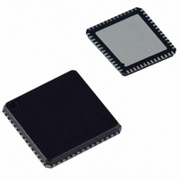
AD9995KCP Analog Devices Inc, AD9995KCP Datasheet - Page 13

AD9995KCP
Manufacturer Part Number
AD9995KCP
Description
IC CCD SIGNAL PROCESSOR 56-LFCSP
Manufacturer
Analog Devices Inc
Type
CCD Signal Processor, 12-Bitr
Datasheet
1.AD9995KCPZRL.pdf
(60 pages)
Specifications of AD9995KCP
Rohs Status
RoHS non-compliant
Input Type
Logic
Output Type
Logic
Interface
3-Wire Serial
Current - Supply
30mA
Mounting Type
Surface Mount
Package / Case
56-LFCSP
Analog Front End Type
CCD
Analog Front End Category
Video
Interface Type
Serial (3-Wire)
Input Voltage Range
0.5V
Operating Supply Voltage (min)
2.7V
Operating Supply Voltage (typ)
3V
Operating Supply Voltage (max)
3.6V
Resolution
12b
Number Of Adc's
1
Power Supply Type
Analog/Digital
Operating Temp Range
-20C to 85C
Operating Temperature Classification
Commercial
Mounting
Surface Mount
Pin Count
56
Package Type
LFCSP EP
Number Of Channels
1
Lead Free Status / RoHS Status
Not Compliant
Available stocks
Company
Part Number
Manufacturer
Quantity
Price
Company:
Part Number:
AD9995KCP
Manufacturer:
ADI
Quantity:
148
Company:
Part Number:
AD9995KCPZ
Manufacturer:
ADI
Quantity:
24
Company:
Part Number:
AD9995KCPZRL7
Manufacturer:
SANYO
Quantity:
1 170
HORIZONTAL CLAMPING AND BLANKING
The AD9995’s horizontal clamping and blanking pulses are fully
programmable to suit a variety of applications. Individual control
is provided for CLPOB, PBLK, and HBLK during the different
regions of each field. This allows the dark pixel clamping and
blanking patterns to be changed at each stage of the readout in
order to accommodate different image transfer timing and high
speed line shifts.
Individual CLPOB and PBLK Patterns
The AFE horizontal timing consists of CLPOB and PBLK, as
shown in Figure 9. These two signals are independently pro-
grammed using the registers in Table III. SPOL is the start
polarity for the signal, and TOG1 and TOG2 are the first and
second toggle positions of the pulse. Both signals are active low
and should be programmed accordingly.
A separate pattern for CLPOB and PBLK may be programmed
for every 10 V-sequences. As described in the Vertical Timing
Generation section, up to 10 separate V-sequences can be created,
Register
SPOL
TOG1
TOG2
Register
HBLKMASK
HBLKALT
HBLKTOG1
HBLKTOG2
HBLKTOG3
HBLKTOG4
HBLKTOG5
HBLKTOG6
REV. 0
CLPOB
PBLK
HD
NOTES
PROGRAMMABLE SETTINGS:
1. START POLARITY (CLAMP AND BLANK REGION ARE ACTIVE LOW)
2. FIRST TOGGLE POSITION
3. SECOND TOGGLE POSITION
(1)
Length
1b
12b
12b
Length
1b
2b
12b
12b
12b
12b
12b
12b
(2)
ACTIVE
Range
High/Low
0–4095 Pixel Location
0–4095 Pixel Location
Range
High/Low
0–3 Alternation Mode
0–4095 Pixel Location
0–4095 Pixel Location
0–4095 Pixel Location
0–4095 Pixel Location
0–4095 Pixel Location
0–4095 Pixel Location
(3)
Figure 9. Clamp and Pre-Blank Pulse Placement
Table III. CLPOB and PBLK Pattern Registers
Table IV. HBLK Pattern Registers
–13–
Description
Starting Polarity of CLPOB/PBLK for V-Sequence 0–9
First Toggle Position within Line for V-Sequence 0–9
Second Toggle Position within Line for V-Sequence 0–9
Description
Masking Polarity for H1/H3 (0 = H1/H3 Low, 1 = H1/H3 High)
Enables Odd/Even Alternation of HBLK Toggle Positions 0 =
Disable Alternation. 1 = TOG1–TOG2 Odd, TOG3–TOG6 Even.
2 = 3 = TOG1–TOG2 Even, TOG3–TOG6 Odd
First Toggle Position within Line for Each V-Sequence 0–9
Second Toggle Position within Line for Each V-Sequence 0–9
Third Toggle Position within Line for Each V-Sequence 0–9
Fourth Toggle Position within Line for Each V-Sequence 0–9
Fifth Toggle Position within Line for Each V-Sequence 0–9
Sixth Toggle Position within Line for Each V-Sequence 0–9
each containing a unique pulse pattern for CLPOB and PBLK.
Figure 9 shows how the sequence change positions divide the
readout field into different regions. A different V-sequence can be
assigned to each region, allowing the CLPOB and PBLK signals
to be changed accordingly with each change in the vertical timing.
Individual HBLK Patterns
The HBLK programmable timing shown in Figure 10 is simi-
lar to CLPOB and PBLK. However, there is no start polarity
control. Only the toggle positions are used to designate the start
and stop positions of the blanking period. Additionally, there is a
polarity control HBLKMASK that designates the polarity of the
horizontal clock signals H1–H4 during the blanking period. Set-
ting HBLKMASK high will set H1 = H3 = low and H2 = H4 =
high during the blanking, as shown in Figure 11. As with the
CLPOB and PBLK signals, HBLK registers are available in each
V-sequence, allowing different blanking signals to be used with
different vertical timing sequences.
ACTIVE
AD9995
. . .
. . .


