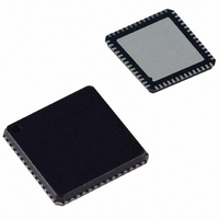
AD9995KCP Analog Devices Inc, AD9995KCP Datasheet - Page 33

AD9995KCP
Manufacturer Part Number
AD9995KCP
Description
IC CCD SIGNAL PROCESSOR 56-LFCSP
Manufacturer
Analog Devices Inc
Type
CCD Signal Processor, 12-Bitr
Datasheet
1.AD9995KCPZRL.pdf
(60 pages)
Specifications of AD9995KCP
Rohs Status
RoHS non-compliant
Input Type
Logic
Output Type
Logic
Interface
3-Wire Serial
Current - Supply
30mA
Mounting Type
Surface Mount
Package / Case
56-LFCSP
Analog Front End Type
CCD
Analog Front End Category
Video
Interface Type
Serial (3-Wire)
Input Voltage Range
0.5V
Operating Supply Voltage (min)
2.7V
Operating Supply Voltage (typ)
3V
Operating Supply Voltage (max)
3.6V
Resolution
12b
Number Of Adc's
1
Power Supply Type
Analog/Digital
Operating Temp Range
-20C to 85C
Operating Temperature Classification
Commercial
Mounting
Surface Mount
Pin Count
56
Package Type
LFCSP EP
Number Of Channels
1
Lead Free Status / RoHS Status
Not Compliant
Available stocks
Company
Part Number
Manufacturer
Quantity
Price
Company:
Part Number:
AD9995KCP
Manufacturer:
ADI
Quantity:
148
Company:
Part Number:
AD9995KCPZ
Manufacturer:
ADI
Quantity:
24
Company:
Part Number:
AD9995KCPZRL7
Manufacturer:
SANYO
Quantity:
1 170
POWER-UP AND SYNCHRONIZATION
Recommended Power-Up Sequence for Master Mode
When the AD9995 is powered up, the following sequence is
recommended (refer to Figure 35 for each step). Note that a
SYNC signal is required for Master mode operation. If an exter-
nal SYNC pulse is not available, it is also possible generate an
internal SYNC pulse by writing to the SYNCPOL register, as
described in the next section.
10. Configure the AD9995 for Master mode timing by writing a
(OUTPUT)
(OUTPUT)
OUTPUTS
REV. 0
1. Turn on power supplies for AD9995.
2. Apply the master clock input CLI.
3. Reset the internal AD9995 registers by writing a 1 to the
4. By default, the AD9995 is in Standby3 mode. To place the
5. Write a 1 to the BANKSELECT register (Addr. 0x7F).
6. Load Bank 2 registers with the required VPAT group,
7. Write a 0 to the BANKSELECT register to select Bank 1.
8. By default, the internal timing core is held in a reset state
9. Load the required registers to configure the high speed tim-
DIGITAL
WRITES
(INPUT)
(INPUT)
SERIAL
(INPUT)
SYNC
VDD
CLI
HD
SW_RESET register (Addr. 0x10 in Bank 1).
part into normal power operation, write 0x004 to the AFE
OPRMODE register (Addr. 0x00 in Bank 1).
This will select Register Bank 2.
V-sequence, and field timing information.
with TGCORE_RSTB register = 0. Write a 1 to the TG-
CORE_RSTB register (Addr. 0x15 in Bank 1) to start the
internal timing core operation.
ing, horizontal timing, and shutter timing information.
1 to the MASTER register (Addr. 0x20 in Bank 1).
VD
1
2
t
PWR
H2/H4
H1/H3, RG, DCLK
Figure 35. Recommended Power-Up Sequence and Synchronization, Master Mode
3
4
5
6
7
8
–33–
11. Write a 1 to the OUT_CONTROL register (Addr. 0x11 in
12. Generate a SYNC event: If SYNC is high at power-up,
Address
0x10
0x00
0x7F
0x00–0xFF
0x7F
0x15
0x30–71
0x20
0x11
0x13
Generating Software SYNC without External SYNC Signal
If an external SYNC pulse is not available, it is possible to
generate an internal SYNC in the AD9995 by writing to the
SYNCPOL register (Addr. 0x13). If the software SYNC option is
used, the SYNC input (Pin 46) should be tied to ground (VSS).
After power-up, follow the same procedure as before for Steps
1 to 11. Then, for Step 12, instead of using the external SYNC
pulse, write a 1 to the SYNCPOL register. This will generate the
SYNC internally, and timing operation will begin.
9
Bank 1). This will allow the outputs to become active after
the next SYNC rising edge.
bring the SYNC input low for a minimum of 100 ns.
Then bring SYNC back high. This will cause the internal
counters to reset and will start VD/HD operation. The first
VD/HD edge allows most Bank 1 register updates to occur,
including OUT_CONTROL to enable all outputs.
Table XIII. Power-Up Register Write Sequence
10
11
Data
0x01
0x04
0x01
0x00
0x01
0x01
0x01
0x01
12
t
SYNC
VPAT, V-Sequence, and Field Timing
1H
Description
Reset All Registers to Default Values
Power Up the AFE and CLO Oscillator
Select Register Bank 2
Select Register Bank 1
Reset Internal Timing Core
Horizontal and Shutter Timing
Configure for Master Mode
Enable All Outputs after SYNC
SYNCPOL (for Software SYNC Only)
CLOCKS ACTIVE WHEN OUT CONTROL
REGISTER IS UPDATED AT VD/HD EDGE
1ST FIELD
1V
AD9995


