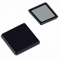
AD9995KCP Analog Devices Inc, AD9995KCP Datasheet - Page 24

AD9995KCP
Manufacturer Part Number
AD9995KCP
Description
IC CCD SIGNAL PROCESSOR 56-LFCSP
Manufacturer
Analog Devices Inc
Type
CCD Signal Processor, 12-Bitr
Datasheet
1.AD9995KCPZRL.pdf
(60 pages)
Specifications of AD9995KCP
Rohs Status
RoHS non-compliant
Input Type
Logic
Output Type
Logic
Interface
3-Wire Serial
Current - Supply
30mA
Mounting Type
Surface Mount
Package / Case
56-LFCSP
Analog Front End Type
CCD
Analog Front End Category
Video
Interface Type
Serial (3-Wire)
Input Voltage Range
0.5V
Operating Supply Voltage (min)
2.7V
Operating Supply Voltage (typ)
3V
Operating Supply Voltage (max)
3.6V
Resolution
12b
Number Of Adc's
1
Power Supply Type
Analog/Digital
Operating Temp Range
-20C to 85C
Operating Temperature Classification
Commercial
Mounting
Surface Mount
Pin Count
56
Package Type
LFCSP EP
Number Of Channels
1
Lead Free Status / RoHS Status
Not Compliant
Available stocks
Company
Part Number
Manufacturer
Quantity
Price
Company:
Part Number:
AD9995KCP
Manufacturer:
ADI
Quantity:
148
Company:
Part Number:
AD9995KCPZ
Manufacturer:
ADI
Quantity:
24
Company:
Part Number:
AD9995KCPZRL7
Manufacturer:
SANYO
Quantity:
1 170
VERTICAL TIMING EXAMPLE
To better understand how the AD9995’s vertical timing generation
is used, consider the example CCD timing chart in Figure 25. This
particular example illustrates a CCD using a general 3-field
readout technique. As described in the Field section, each
readout field should be divided into separate regions to per-
form each step of the readout. The sequence change positions
(SCP) determine the line boundaries for each region, and the
VSEQSEL registers will then assign a particular V-sequence to
each region. The V-sequences will contain the specific timing
information required in each region: V1–V6 pulses (using VPAT
groups), HBLK/CLPOB timing, and VSG patterns for the SG
active lines.
This particular timing example requires four regions for each
of the three fields, labeled Region 0, Region 1, Region 2, and
Region 3. Because the AD9995 allows up to six individual fields
to be programmed, the Field 0, Field 1, and Field 2 registers can
be used to meet the requirements of this timing example. The
four regions for each field are very similar in this example, but
the individual registers for each field allow flexibility to accom-
modate other timing charts.
Region 0 is a high speed vertical shift region. Sweep mode can be
used to generate this timing operation, with the desired number
of high speed vertical pulses needed to clear any charge from the
CCD’s vertical registers.
AD9995
–24–
Region 1 consists of only two lines, and uses standard single line
vertical shift timing. The timing of this region area will be the
same as the timing in Region 3.
Region 2 is the sensor gate line, where the VSG pulses transfer the
image into the vertical CCD registers. This region may require the
use of the second V-pattern group for SG active line.
Region 3 also uses the standard single line vertical shift timing,
the same timing as Region 1.
In summary, four regions are required in each of the three fields.
The timing for Regions 1 and 3 is essentially the same, reducing
the complexity of the register programming.
Other registers will need to be used during the actual readout
operation, such as the MODE register, shutter control registers
(TRIGGER, SUBCK, VSUB, MSHUT, STROBE), and AFE
gain register. These registers will be explained in other examples.
Important Note about Signal Polarities
When programming the AD9995 to generate the V1–V6,
VSG1–VSG5, and SUBCK signals, it is important to note that
the V-driver circuit usually inverts these signals. Carefully check
the required timing signals needed at the input and output of
the V-driver circuit being used and adjust the polarities of the
AD9995’s outputs accordingly.
REV. 0


