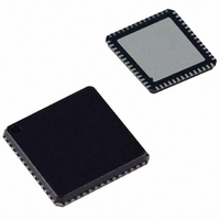
AD9995KCP Analog Devices Inc, AD9995KCP Datasheet - Page 16

AD9995KCP
Manufacturer Part Number
AD9995KCP
Description
IC CCD SIGNAL PROCESSOR 56-LFCSP
Manufacturer
Analog Devices Inc
Type
CCD Signal Processor, 12-Bitr
Datasheet
1.AD9995KCPZRL.pdf
(60 pages)
Specifications of AD9995KCP
Rohs Status
RoHS non-compliant
Input Type
Logic
Output Type
Logic
Interface
3-Wire Serial
Current - Supply
30mA
Mounting Type
Surface Mount
Package / Case
56-LFCSP
Analog Front End Type
CCD
Analog Front End Category
Video
Interface Type
Serial (3-Wire)
Input Voltage Range
0.5V
Operating Supply Voltage (min)
2.7V
Operating Supply Voltage (typ)
3V
Operating Supply Voltage (max)
3.6V
Resolution
12b
Number Of Adc's
1
Power Supply Type
Analog/Digital
Operating Temp Range
-20C to 85C
Operating Temperature Classification
Commercial
Mounting
Surface Mount
Pin Count
56
Package Type
LFCSP EP
Number Of Channels
1
Lead Free Status / RoHS Status
Not Compliant
Available stocks
Company
Part Number
Manufacturer
Quantity
Price
Company:
Part Number:
AD9995KCP
Manufacturer:
ADI
Quantity:
148
Company:
Part Number:
AD9995KCPZ
Manufacturer:
ADI
Quantity:
24
Company:
Part Number:
AD9995KCPZRL7
Manufacturer:
SANYO
Quantity:
1 170
VERTICAL TIMING GENERATION
The AD9995 provides a very flexible solution for generating
vertical CCD timing, and can support multiple CCDs and dif-
ferent system architectures. The 6-phase vertical transfer clocks
V1–V6 are used to shift each line of pixels into the horizontal
output register of the CCD. The AD9995 allows these outputs to
be individually programmed into various readout configurations
using a 4-step process.
Figure 15 shows an overview of how the vertical timing is gener-
ated in four steps. First, the individual pulse patterns for V1–V6
AD9995
VPAT 9
VPAT 0
FIELD 0
FIELD 3
FIELD 5
CREATE THE VERTICAL PATTERN GROUPS
(MAXIMUM OF 10 GROUPS).
USE THE MODE REGISTER TO CONTROL WHICH FIELDS
ARE USED, AND IN WHAT ORDER
(MAXIMUM OF 7 FIELDS MAY BE COMBINED IN ANY ORDER).
V3
V1
V2
V4
V5
V6
V1
V2
V3
V4
V5
V6
FIELD 1
FIELD 4
FIELD 1
Figure 15. Summary of VerticalTiming Generation
FIELD 2
FIELD 4
FIELD 2
–16–
are created by using the vertical pattern group registers. Second,
the V-pattern groups are used to build the sequences, where
additional information is added. Third, the readout for an entire
field is constructed by dividing the field into different regions and
then assigning a sequence to each region. Each field can contain
up to seven different regions to accommodate different steps of
the readout such as high speed line shifts and unique vertical line
transfers. Up to six different fields may be created. Finally, the
Mode register allows the different fields to be combined into any
order for various readout configurations.
V-SEQUENCE 2
(VPAT9, N REP)
V-SEQUENCE 0
(VPAT0, 1 REP)
V-SEQUENCE 1
(VPAT9, 2 REP)
FIELD 0
BUILD EACH FIELD BY DIVIDING INTO DIFFERENT REGIONS,
AND ASSIGNING A DIFFERENT V-SEQUENCE TO EACH
(MAXIMUM OF 7 REGIONS IN EACH FIELD)
(MAXIMUM OF 6 FIELDS).
FIELD 1
BUILD THE V-SEQUENCES BY ADDING LINE START
POSITION, # OF REPEATS, AND HBLK/CLPOB PULSES
(MAXIMUM OF 10 V-SEQUENCES).
FIELD 2
REGION 0: USE V-SEQUENCE 2
REGION 1: USE V-SEQUENCE 0
REGION 2: USE V-SEQUENCE 3
REGION 3: USE V-SEQUENCE 0
REGION 4: USE V-SEQUENCE 2
V3
V1
V2
V4
V5
V6
V3
V1
V2
V3
V4
V5
V6
V1
V2
V4
V5
V6
REGION 0: USE V-SEQUENCE 3
REGION 1: USE V-SEQUENCE 2
REGION 2: USE V-SEQUENCE 1
REGION 0: USE V-SEQUENCE 3
REGION 1: USE V-SEQUENCE 2
REGION 2: USE V-SEQUENCE 1
REV. 0


