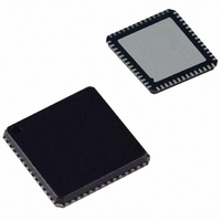
AD9995KCP Analog Devices Inc, AD9995KCP Datasheet - Page 11

AD9995KCP
Manufacturer Part Number
AD9995KCP
Description
IC CCD SIGNAL PROCESSOR 56-LFCSP
Manufacturer
Analog Devices Inc
Type
CCD Signal Processor, 12-Bitr
Datasheet
1.AD9995KCPZRL.pdf
(60 pages)
Specifications of AD9995KCP
Rohs Status
RoHS non-compliant
Input Type
Logic
Output Type
Logic
Interface
3-Wire Serial
Current - Supply
30mA
Mounting Type
Surface Mount
Package / Case
56-LFCSP
Analog Front End Type
CCD
Analog Front End Category
Video
Interface Type
Serial (3-Wire)
Input Voltage Range
0.5V
Operating Supply Voltage (min)
2.7V
Operating Supply Voltage (typ)
3V
Operating Supply Voltage (max)
3.6V
Resolution
12b
Number Of Adc's
1
Power Supply Type
Analog/Digital
Operating Temp Range
-20C to 85C
Operating Temperature Classification
Commercial
Mounting
Surface Mount
Pin Count
56
Package Type
LFCSP EP
Number Of Channels
1
Lead Free Status / RoHS Status
Not Compliant
Available stocks
Company
Part Number
Manufacturer
Quantity
Price
Company:
Part Number:
AD9995KCP
Manufacturer:
ADI
Quantity:
148
Company:
Part Number:
AD9995KCPZ
Manufacturer:
ADI
Quantity:
24
Company:
Part Number:
AD9995KCPZRL7
Manufacturer:
SANYO
Quantity:
1 170
mapped into four quadrants, with each quadrant containing 12
edge locations. Table II shows the correct register values for the
corresponding edge locations.
Figure 7 shows the default timing locations for all of the high
speed clock signals.
H-Driver and RG Outputs
In addition to the programmable timing positions, the AD9995
features on-chip output drivers for the RG and H1–H4 outputs.
These drivers are powerful enough to directly drive the CCD
inputs. The H-driver and RG current can be adjusted for optimum
rise/fall time into a particular load by using the DRVCONTROL
register (Addr. 0x35). The 3-bit drive setting for each output is
adjustable in 4.1 mA increments, with the minimum setting of 0
equal to OFF or three-state, and the maximum setting of 7 equal
to 30.1 mA.
As shown in Figures 5, 6, and 7, the H2 and H4 outputs are
inverses of H1 and H3, respectively. The H1/H2 crossover volt-
age is approximately 50% of the output swing. The crossover
voltage is not programmable.
Parameter
Polarity
Positive Edge
Negative Edge
Sampling Location
Drive Strength
Quadrant
I
II
III
IV
REV. 0
SIGNAL
USING THE SAME TOGGLE POSITIONS FOR H1 AND H3 GENERATES STANDARD 2-PHASE H-CLOCKING.
H1/H3
H2/H4
CCD
RG
Length
1b
6b
6b
6b
3b
Table I. Timing Core Register Parameters for H1, H3, RG, SHP/SHD
Edge Location (Dec)
0 to 11
12 to 23
24 to 35
36 to 47
Range
High/Low
0–47 Edge Location
0–47 Edge Location
0–47 Edge Location
0–47 Current Steps
Table II. Precision Timing Edge Locations
Figure 6. 2-Phase H-Clock Operation
Description
Polarity Control for H1, H3, and RG (0 = No Inversion, 1 = Inversion)
Positive Edge Location for H1, H3, and RG
Negative Edge Location for H1, H3, and RG
Sampling Location for Internal SHP and SHD Signals
Drive Current for H1–H4 and RG Outputs (4.1 mA per Step)
–11–
Digital Data Outputs
The AD9995 data output and DCLK phases are programmable
using the DOUTPHASE register (Addr. 0x37, Bits [5:0]). Any
edge from 0 to 47 may be programmed, as shown in Figure 8a.
Normally, the DOUT and DCLK signals will track in phase
based on the DOUTPHASE register contents. The DCLK
output phase can also be held fixed with respect to the data out-
puts by changing the DCLKMODE register high (Addr. 0x37,
Bit 6). In this mode, the DCLK output will remain at a fixed
phase equal to CLO (the inverse of CLI) while the data output
phase is still programmable.
There is a fixed output delay from the DCLK rising edge to the
DOUT transition, called t
four values between 0 ns and 12 ns by using the DOUTDELAY
register (Addr. 0x037, Bits [8:7]). The default value is 8 ns.
The pipeline delay through the AD9995 is shown in Figure 8b.
After the CCD input is sampled by SHD, there is an 11-cycle
delay until the data is available.
Register Value (Dec)
0 to 11
16 to 27
32 to 43
48 to 59
OD
. This delay can be programmed to
Register Value (Bin)
000000 to 001011
010000 to 011011
100000 to 101011
110000 to 111011
AD9995


