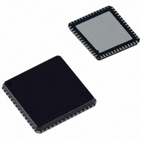
AD9995KCP Analog Devices Inc, AD9995KCP Datasheet - Page 21

AD9995KCP
Manufacturer Part Number
AD9995KCP
Description
IC CCD SIGNAL PROCESSOR 56-LFCSP
Manufacturer
Analog Devices Inc
Type
CCD Signal Processor, 12-Bitr
Datasheet
1.AD9995KCPZRL.pdf
(60 pages)
Specifications of AD9995KCP
Rohs Status
RoHS non-compliant
Input Type
Logic
Output Type
Logic
Interface
3-Wire Serial
Current - Supply
30mA
Mounting Type
Surface Mount
Package / Case
56-LFCSP
Analog Front End Type
CCD
Analog Front End Category
Video
Interface Type
Serial (3-Wire)
Input Voltage Range
0.5V
Operating Supply Voltage (min)
2.7V
Operating Supply Voltage (typ)
3V
Operating Supply Voltage (max)
3.6V
Resolution
12b
Number Of Adc's
1
Power Supply Type
Analog/Digital
Operating Temp Range
-20C to 85C
Operating Temperature Classification
Commercial
Mounting
Surface Mount
Pin Count
56
Package Type
LFCSP EP
Number Of Channels
1
Lead Free Status / RoHS Status
Not Compliant
Available stocks
Company
Part Number
Manufacturer
Quantity
Price
Company:
Part Number:
AD9995KCP
Manufacturer:
ADI
Quantity:
148
Company:
Part Number:
AD9995KCPZ
Manufacturer:
ADI
Quantity:
24
Company:
Part Number:
AD9995KCPZRL7
Manufacturer:
SANYO
Quantity:
1 170
Sweep Mode Operation
The AD9995 contains an additional mode of vertical timing
operation called Sweep mode. This mode is used to generate a
large number of repetitive pulses that span multiple HD lines.
One example of where this mode is needed is at the start of the
CCD readout operation. At the end of the image exposure but
before the image is transferred by the sensor gate pulses, the
vertical interline CCD registers should be free of all charge. This
can be accomplished by quickly shifting out any charge using a
long series of pulses from the V1–V6 outputs. Depending on the
vertical resolution of the CCD, up to 2,000 or 3,000 clock cycles
will be needed to shift the charge out of each vertical CCD line.
This operation will span across multiple HD line lengths. Nor-
mally, the AD9995’s vertical timing must be contained within
one HD line length, but when Sweep mode is enabled, the HD
boundaries will be ignored until the region is finished. To enable
Sweep mode within any region, program the appropriate
SWEEP register to high.
Figure 21 shows an example of Sweep mode operation. The
number of vertical pulses needed will depend on the vertical
resolution of the CCD. The V1–V6 output signals are gener-
ated using the V-pattern registers (shown in Table VII). A single
pulse is created using the polarity and toggle position registers.
The number of repetitions is then programmed to match the
number of vertical shifts required by the CCD. Repetitions are
programmed in the V-sequence registers using the VPATREP
registers. This produces a pulse train of the appropriate length.
Normally, the pulse train would be truncated at the end of the
HD line length, but with Sweep mode enabled for this region,
the HD boundaries will be ignored. In Figure 21, the Sweep
Register
MULTI
VPOL
VTOG1
VTOG2
VTOG3
VPATLEN
VPATREP
REV. 0
V1–V6
HD
VD
Length
1b
1b
12b
12b
12b
10b
12b
LINE 0
0
REGION 0
Figure 21. Example of Sweep Region for High Speed Vertical Shift
Range
High/Low
High/Low
0–4095 Pixel Location
0–4095 Pixel Location
0–4095 Pixel Location
0–1023 Pixels
0–4096
L
LINE 1
Table VIII. Multiplier Mode Register Parameters
SCP 1
LINE 2
Description
High enables Multiplier mode.
Starting Polarity of V1–V6 Signal in Each VPAT Group.
First Toggle Position for V1–V6 Signal in Each VPAT Group.
Second Toggle Position for V1–V6 Signal in Each VPAT Group.
Third Toggle Position for V1–V6 Signal in Each VPAT Group.
Used as Multiplier Factor for Toggle Position Counter.
VPATREPE/VPATREPO should be set to the same value as TOG2 or 3.
–21–
REGION 1: SWEEP REGION
region occupies 23 HD lines. After the Sweep mode region is
completed, in the next region, normal sequence operation will
resume. When using Sweep mode, be sure to set the region
boundaries (using the sequence change positions) to the appro-
priate lines to prevent the Sweep operation from overlapping the
next V-sequence.
Multiplier Mode
To generate very wide vertical timing pulses, a vertical region
may be configured into a multiplier region. This mode uses
the V-pattern registers in a slightly different manner. Multiplier
mode can be used to support unusual CCD timing requirements,
such as vertical pulses that are wider than a single HD line length.
The start polarity and toggle positions are still used in the same
manner as the standard VPAT group programming, but the
VPATLEN is used differently. Instead of using the pixel counter
(HD counter) to specify the toggle position locations (VTOG1,
2, 3) of the VPAT group, the VPATLEN is multiplied with the
VTOG position to allow very long pulses to be generated. To cal-
culate the exact toggle position, counted in pixels after the start
position, use the equation
Because the VTOG register is multiplied by VPATLEN,
the resolution of the toggle position placement is reduced. If
VPATLEN = 4, the toggle position accuracy is now reduced
to 4-pixel steps instead of single pixel steps. Table VIII sum-
marizes how the VPAT group registers are used in Multiplier
mode operation. In Multiplier mode, the VPATREPO and
VPATREPE registers should always be programmed to the same
value as the highest toggle position.
Multiplier ModeTogglePosition VTOG VPATLEN
LINE 24
SCP 2
=
LINE 25
REGION 2
×
AD9995


