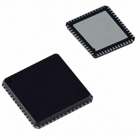
AD9995KCP Analog Devices Inc, AD9995KCP Datasheet - Page 38

AD9995KCP
Manufacturer Part Number
AD9995KCP
Description
IC CCD SIGNAL PROCESSOR 56-LFCSP
Manufacturer
Analog Devices Inc
Type
CCD Signal Processor, 12-Bitr
Datasheet
1.AD9995KCPZRL.pdf
(60 pages)
Specifications of AD9995KCP
Rohs Status
RoHS non-compliant
Input Type
Logic
Output Type
Logic
Interface
3-Wire Serial
Current - Supply
30mA
Mounting Type
Surface Mount
Package / Case
56-LFCSP
Analog Front End Type
CCD
Analog Front End Category
Video
Interface Type
Serial (3-Wire)
Input Voltage Range
0.5V
Operating Supply Voltage (min)
2.7V
Operating Supply Voltage (typ)
3V
Operating Supply Voltage (max)
3.6V
Resolution
12b
Number Of Adc's
1
Power Supply Type
Analog/Digital
Operating Temp Range
-20C to 85C
Operating Temperature Classification
Commercial
Mounting
Surface Mount
Pin Count
56
Package Type
LFCSP EP
Number Of Channels
1
Lead Free Status / RoHS Status
Not Compliant
Available stocks
Company
Part Number
Manufacturer
Quantity
Price
Company:
Part Number:
AD9995KCP
Manufacturer:
ADI
Quantity:
148
Company:
Part Number:
AD9995KCPZ
Manufacturer:
ADI
Quantity:
24
Company:
Part Number:
AD9995KCPZRL7
Manufacturer:
SANYO
Quantity:
1 170
Register Address Banks 1 and 2
The AD9995 address space is divided into two different regis-
ter banks, referred to as Register Bank 1 and Register Bank 2.
Figure 41 illustrates how the two banks are divided. Register
Bank 1 contains the registers for the AFE, miscellaneous func-
tions, VD/HD parameters, timing core, CLPOB masking, VSG
patterns, and shutter functions. Register Bank 2 contains all
of the information for the V-pattern groups, V-sequences, and
field information.
AD9995
ADDR 0xFF
ADDR 0x8F
ADDR 0x00
ADDR 0x10
ADDR 0x20
ADDR 0x30
ADDR 0x40
ADDR 0x50
ADDR 0x60
ADDR 0x7F
MISCELLANEOUS REGISTERS
SWITCH TO REGISTER BANK 2
VSG PATTERN REGISTERS
INVALID—DO NOT ACCESS
CLPOB MASK REGISTERS
TIMING CORE REGISTERS
SHUTTER REGISTERS
REGISTER BANK 1
VD/HD REGISTERS
AFE REGISTERS
Figure 41. Layout of Internal Register Banks 1 and 2
WRITE TO ADDRESS 0x7F TO SWITCH REGISTER BANKS
–38–
When writing to the AD9995, Address 0x7F is used to specify
which address bank is being written to. To write to Bank 1, the
LSB of Address 0x7F should be set to 0; to write to Bank 2, the
LSB of Address 0x7F should be set to 1.
Note that Register Bank 1 contains many unused addresses. Any
undefined addresses between 0x00 and 0x7F are considered
don’t cares, and it is acceptable if these addresses are filled in
with all 0s during a continuous register write operation. However,
the undefined addresses above 0x7F must not be written to, or
the AD9995 may not operate properly.
ADDR 0x00
ADDR 0x7E
ADDR 0x7F
ADDR 0x80
ADDR 0xCF
ADDR 0xD0
ADDR 0xFF
SWITCH TO REGISTER BANK 1
FIELD 0–FIELD 5 REGISTERS
VSEQ0–VSEQ9 REGISTERS
VPAT0–VPAT9 REGISTERS
REGISTER BANK 2
REV. 0


