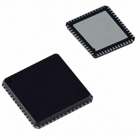
AD9995KCP Analog Devices Inc, AD9995KCP Datasheet - Page 9

AD9995KCP
Manufacturer Part Number
AD9995KCP
Description
IC CCD SIGNAL PROCESSOR 56-LFCSP
Manufacturer
Analog Devices Inc
Type
CCD Signal Processor, 12-Bitr
Datasheet
1.AD9995KCPZRL.pdf
(60 pages)
Specifications of AD9995KCP
Rohs Status
RoHS non-compliant
Input Type
Logic
Output Type
Logic
Interface
3-Wire Serial
Current - Supply
30mA
Mounting Type
Surface Mount
Package / Case
56-LFCSP
Analog Front End Type
CCD
Analog Front End Category
Video
Interface Type
Serial (3-Wire)
Input Voltage Range
0.5V
Operating Supply Voltage (min)
2.7V
Operating Supply Voltage (typ)
3V
Operating Supply Voltage (max)
3.6V
Resolution
12b
Number Of Adc's
1
Power Supply Type
Analog/Digital
Operating Temp Range
-20C to 85C
Operating Temperature Classification
Commercial
Mounting
Surface Mount
Pin Count
56
Package Type
LFCSP EP
Number Of Channels
1
Lead Free Status / RoHS Status
Not Compliant
Available stocks
Company
Part Number
Manufacturer
Quantity
Price
Company:
Part Number:
AD9995KCP
Manufacturer:
ADI
Quantity:
148
Company:
Part Number:
AD9995KCPZ
Manufacturer:
ADI
Quantity:
24
Company:
Part Number:
AD9995KCPZRL7
Manufacturer:
SANYO
Quantity:
1 170
SYSTEM OVERVIEW
Figure 1 shows the typical system block diagram for the AD9995
used in Master mode. The CCD output is processed by the
AD9995’s AFE circuitry, which consists of a CDS, VGA, black
level clamp, and A/D converter. The digitized pixel information
is sent to the digital image processor chip, which performs the
postprocessing and compression. To operate the CCD, all CCD
timing parameters are programmed into the AD9995 from the
system microprocessor through the 3-wire serial interface. From
the system master clock, CLI, provided by the image processor
or external crystal, the AD9995 generates all of the CCD’s hori-
zontal and vertical clocks and all internal AFE clocks. External
synchronization is provided by a SYNC pulse from the micropro-
cessor, which will reset internal counters and resync the VD and
HD outputs.
Alternatively, the AD9995 may be operated in Slave mode, in
which VD and HD are provided externally from the image pro-
cessor. In this mode, all AD9995 timing will be synchronized
with VD and HD.
REV. 0
Figure 1.Typical System Block Diagram, Master Mode
CCD
CLI
VD
HD
H1–H4, RG, VSUB
STROBE
V-DRIVER
MSHUT
CCDIN
SYNC
MAX VD LENGTH IS 4095 LINES
V1–V6, VSG1–VSG5, SUBCK
AD9995
AFETG
SERIAL
INTERFACE
HD, VD
DOUT
DCLK
CLI
MAX HD LENGTH IS 4095 PIXELS
Figure 3. Maximum VD/HD Dimensions
PROCESSING
DIGITAL
IMAGE
ASIC
–9–
The H-drivers for H1–H4 and RG are included in the AD9995,
allowing these clocks to be directly connected to the CCD.
H-drive voltage of up to 3.3 V is supported. An external V-driver
is required for the vertical transfer clocks, the sensor gate pulses,
and the substrate clock.
The AD9995 also includes programmable MSHUT and
STROBE outputs, which may be used to trigger mechanical
shutter and strobe (flash) circuitry.
Figures 2 and 3 show the maximum horizontal and vertical
counter dimensions for the AD9995. All internal horizontal and
vertical clocking is controlled by these counters to specify line
and pixel locations. Maximum HD length is 4095 pixels per line,
and maximum VD length is 4095 lines per field.
Figure 2. Vertical and Horizontal Counters
MAXIMUM
FIELD
DIMENSIONS
12-BIT HORIZONTAL = 4096 PIXELS MAX
12-BIT VERTICAL = 4096 LINES MAX
AD9995


