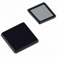
AD9995KCP Analog Devices Inc, AD9995KCP Datasheet - Page 40

AD9995KCP
Manufacturer Part Number
AD9995KCP
Description
IC CCD SIGNAL PROCESSOR 56-LFCSP
Manufacturer
Analog Devices Inc
Type
CCD Signal Processor, 12-Bitr
Datasheet
1.AD9995KCPZRL.pdf
(60 pages)
Specifications of AD9995KCP
Rohs Status
RoHS non-compliant
Input Type
Logic
Output Type
Logic
Interface
3-Wire Serial
Current - Supply
30mA
Mounting Type
Surface Mount
Package / Case
56-LFCSP
Analog Front End Type
CCD
Analog Front End Category
Video
Interface Type
Serial (3-Wire)
Input Voltage Range
0.5V
Operating Supply Voltage (min)
2.7V
Operating Supply Voltage (typ)
3V
Operating Supply Voltage (max)
3.6V
Resolution
12b
Number Of Adc's
1
Power Supply Type
Analog/Digital
Operating Temp Range
-20C to 85C
Operating Temperature Classification
Commercial
Mounting
Surface Mount
Pin Count
56
Package Type
LFCSP EP
Number Of Channels
1
Lead Free Status / RoHS Status
Not Compliant
Available stocks
Company
Part Number
Manufacturer
Quantity
Price
Company:
Part Number:
AD9995KCP
Manufacturer:
ADI
Quantity:
148
Company:
Part Number:
AD9995KCPZ
Manufacturer:
ADI
Quantity:
24
Company:
Part Number:
AD9995KCPZRL7
Manufacturer:
SANYO
Quantity:
1 170
COMPLETE LISTING FOR REGISTER BANK 1
All registers are VD updated, except where noted:
All address and default values are in hexadecimal.
Address Content Value
00
01
02
03
Address Content Value
10
11
12
13
14
15
16
17
18
19
1A
1B
1C
Address Content Value
20
21
22
AD9995
Data Bit Default
[11:0]
[9:0]
[7:0]
[11:0]
Data Bit Default
[0]
[0]
[0]
[0]
[0]
[0]
[0]
[0]
[11:0]
[0]
[23:0]
[1:0]
Data Bit Default
[0]
[0]
[17:0]
7
0
80
4
0
0
1
0
0
0
1
0
0
0
0
0
0
0
0
Register Name
OPRMODE
VGAGAIN
CLAMPLEVEL
CTLMODE
Register Name
SW_RST
OUTCONTROL
TEST USE
SYNCPOL
SYNCSUSPEND
TGCORE_RSTB
OSC_PWRDOWN
TEST USE
UPDATE
PREVENTUPDATE
MODE
FIELDVAL
Register Name
MASTER
VDHDPOL
VDHDRISE
Table XVII. Miscellaneous Register Map
Table XVIII. VD/HD Register Map
Table XVI. AFE Register Map
Register Description
AFE Operation Modes (see Table XXIV for detail).
VGA Gain.
Optical Black Clamp Level.
AFE Control Modes (see Table XXV for detail).
Register Description
Software Reset. 1 = Reset all registers to default, then self-clear back to 0.
Output Control. 0 = Make all outputs dc inactive.
Internal Use Only. Must be set to 1.
SYNC Active Polarity (0 = Active Low).
Suspend Clocks during SYNC Active (1 = Suspend).
Timing Core Reset Bar. 0 = Reset TG Core, 1 = Resume Operation.
CLO Oscillator Power-Down (0 = Oscillator is powered-down).
Unused.
Internal Use Only. Must be set to 0.
Serial Update. Line (HD) in the field to update VD updated registers.
Prevents the Update of the VD Updated Registers. 1 = Prevent update.
Mode Register.
Field Value Sync. 0 = Next Field 0, 1 = Next Field 1, 2/3 = Next Field 2.
Register Description
VD/HD Master or Slave Timing (0 = Slave mode).
VD/HD Active Polarity. 0 = Low, 1 = High.
Rising Edge Location for VD [17:12] and HD [11:0].
= SCK Updated
–40–
= SG-Line Updated
REV. 0


