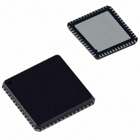
AD9995KCP Analog Devices Inc, AD9995KCP Datasheet - Page 28

AD9995KCP
Manufacturer Part Number
AD9995KCP
Description
IC CCD SIGNAL PROCESSOR 56-LFCSP
Manufacturer
Analog Devices Inc
Type
CCD Signal Processor, 12-Bitr
Datasheet
1.AD9995KCPZRL.pdf
(60 pages)
Specifications of AD9995KCP
Rohs Status
RoHS non-compliant
Input Type
Logic
Output Type
Logic
Interface
3-Wire Serial
Current - Supply
30mA
Mounting Type
Surface Mount
Package / Case
56-LFCSP
Analog Front End Type
CCD
Analog Front End Category
Video
Interface Type
Serial (3-Wire)
Input Voltage Range
0.5V
Operating Supply Voltage (min)
2.7V
Operating Supply Voltage (typ)
3V
Operating Supply Voltage (max)
3.6V
Resolution
12b
Number Of Adc's
1
Power Supply Type
Analog/Digital
Operating Temp Range
-20C to 85C
Operating Temperature Classification
Commercial
Mounting
Surface Mount
Pin Count
56
Package Type
LFCSP EP
Number Of Channels
1
Lead Free Status / RoHS Status
Not Compliant
Available stocks
Company
Part Number
Manufacturer
Quantity
Price
Company:
Part Number:
AD9995KCP
Manufacturer:
ADI
Quantity:
148
Company:
Part Number:
AD9995KCPZ
Manufacturer:
ADI
Quantity:
24
Company:
Part Number:
AD9995KCPZRL7
Manufacturer:
SANYO
Quantity:
1 170
It is possible to independently trigger the readout operation
without triggering the exposure operation. This will cause the
readout to occur at the next VD, and the SUBCK output will be
suppressed according to the value of the READOUT register.
The TRIGGER register is also used to control the STROBE,
MSHUT, and VSUB signal transitions. Each of these signals are
individually controlled, although they will be dependent on the
triggering of the exposure and readout operation.
See Figure 32 for a complete example of triggering the exposure
and readout operations.
VSUB Control
The CCD readout bias (VSUB) can be programmed to accom-
modate different CCDs. Figure 29 shows two different modes
that are available. In Mode 0, VSUB goes active during the field
of the last SUBCK when the exposure begins. The On position
(rising edge in Figure 29) is programmable to any line within
AD9995
SUBCK
SUBCK
MSHUT
VSUB
VSG1
VSG
VD
VD
1
MSHUT PROGRAMMABLE SETTINGS:
1. ACTIVE POLARITY.
2. ON POSITION IS VD UPDATED AND MAY BE SWITCHED ON AT ANY TIME.
3. OFF POSITION CAN BE PROGRAMMED ANYWHERE FROM THE FIELD OF LAST SUBCK UNTIL THE FIELD BEFORE READOUT.
1
VSUB OPERATION:
1. ACTIVE POLARITY IS POLARITY (ABOVE EXAMPLE IS VSUB ACTIVE HIGH).
2. ON POSITION IS PROGRAMMABLE. MODE 0 TURNS ON AT THE START OF EXPOSURE, MODE 1 TURNS ON AT THE START OF READOUT.
3. OFF POSITION OCCURS AT END OF READOUT.
4. OPTIONAL VSUB KEEP-ON MODE WILL LEAVE THE VSUB ACTIVE AT THE END OF READOUT.
TRIGGER
VSUB
2
2
MODE 0
AND MSHUT
EXPOSURE
TRIGGER
Figure 30. MSHUT Output Programmability
Figure 29. VSUB Programmability
t
EXP
MODE 1
–28–
the field. VSUB will remain active until the end of the image
readout. In Mode 1, the VSUB is not activated until the start of
the readout.
An additional function called VSUB KEEP-ON is also available.
When this bit is set high, the VSUB output will remain on (active)
even after the readout has finished.To disable the VSUB at a later
time, set this bit back to low.
MSHUT and STROBE Control
MSHUT and STROBE operation is shown in Figures 30, 31,
and 32. Table XII shows the register parameters for controlling
the MSHUT and STROBE outputs. The MSHUT output is
switched on with the MSHUTON registers, and will remain on
until the location specified in the MSHUTOFF registers. The
location of MSHUTOFF is fully programmable to anywhere
within the exposure period, using the FD (field), LN (line), and
PX (pixel) registers. The STROBE pulse is defined by the on and
2
3
READOUT
t
EXP
3
4
REV. 0


