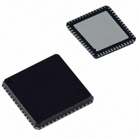
AD9995KCP Analog Devices Inc, AD9995KCP Datasheet - Page 3

AD9995KCP
Manufacturer Part Number
AD9995KCP
Description
IC CCD SIGNAL PROCESSOR 56-LFCSP
Manufacturer
Analog Devices Inc
Type
CCD Signal Processor, 12-Bitr
Datasheet
1.AD9995KCPZRL.pdf
(60 pages)
Specifications of AD9995KCP
Rohs Status
RoHS non-compliant
Input Type
Logic
Output Type
Logic
Interface
3-Wire Serial
Current - Supply
30mA
Mounting Type
Surface Mount
Package / Case
56-LFCSP
Analog Front End Type
CCD
Analog Front End Category
Video
Interface Type
Serial (3-Wire)
Input Voltage Range
0.5V
Operating Supply Voltage (min)
2.7V
Operating Supply Voltage (typ)
3V
Operating Supply Voltage (max)
3.6V
Resolution
12b
Number Of Adc's
1
Power Supply Type
Analog/Digital
Operating Temp Range
-20C to 85C
Operating Temperature Classification
Commercial
Mounting
Surface Mount
Pin Count
56
Package Type
LFCSP EP
Number Of Channels
1
Lead Free Status / RoHS Status
Not Compliant
Available stocks
Company
Part Number
Manufacturer
Quantity
Price
Company:
Part Number:
AD9995KCP
Manufacturer:
ADI
Quantity:
148
Company:
Part Number:
AD9995KCPZ
Manufacturer:
ADI
Quantity:
24
Company:
Part Number:
AD9995KCPZRL7
Manufacturer:
SANYO
Quantity:
1 170
Parameter
TEMPERATURE RANGE
POWER SUPPLY VOLTAGE
POWER DISSIPATION (See TPC 1 for Power Curves)
MAXIMUM CLOCK RATE (CLI)
*The total power dissipated by the HVDD supply may be approximated using the equation
Reducing the H-loading, using only two of the outputs, and/or using a lower HVDD supply will reduce the power dissipation.
Specifications subject to change without notice.
DIGITAL SPECIFICATIONS
Parameter
LOGIC INPUTS
LOGIC OUTPUTS (Except H and RG)
RG and H-DRIVER OUTPUTS (H1–H4)
Specifications subject to change without notice.
AD9995–SPECIFICATIONS
REV. 0
TCVDD (Timing Core Analog Supply)
AVDD (AFE Analog Supply)
Operating
Storage
RGVDD (RG Driver)
HVDD (H1–H4 Drivers)
DRVDD (Data Output Drivers)
DVDD (Digital)
36 MHz, Typ Supply Levels, 100 pF H1–H4 Loading
Power from HVDD Only*
Standby 1 Mode
Standby 2 Mode
Standby 3 Mode
High Level Input Voltage
Low Level Input Voltage
High Level Input Current
Low Level Input Current
Input Capacitance
High Level Output Voltage @ I
Low Level Output Voltage @ I
High Level Output Voltage @ Max Current
Low Level Output Voltage @ Max Current
Maximum Output Current (Programmable)
Maximum Load Capacitance (For Each Output)
Total HVDD Power
=
=
=
=
=
=
=
[
[
[
[
[
[
[
[
[
[
C
C
C
C
C
C
LOAD
LOAD
LOAD
LOAD
LOAD
LOAD
×
×
×
×
×
×
×
HVDD
HVDD
OL
OL
OL
OH
= 2 mA
= 2 mA
= 2 mA
×
×
Pixel
Pixel Frequency
Frequency
]
]
]
]
]
]
]
]
]
]
×
×
HVDD
HVDD
HVDD
×
×
Number of H outputs used
–3–
Symbol
V
V
I
I
C
V
V
V
V
IH
IL
IH
IL
OH
OL
OH
OL
IN
H−
H
−
Min
–20
–65
2.7
2.7
2.7
2.7
2.7
2.7
36
Min
2.1
2.2
VDD – 0.5
30
100
Typ
3.0
3.0
3.0
3.0
3.0
3.0
360
130
130
12
0.5
Typ
10
10
10
Max
+85
+150
3.6
3.6
3.6
3.6
3.6
3.6
Max
0.6
0.5
0.5
V
V
V
Unit
°C
°C
V
V
V
V
V
V
mW
mW
mW
mW
mW
MHz
Unit
V
µA
µA
pF
V
V
mA
pF


