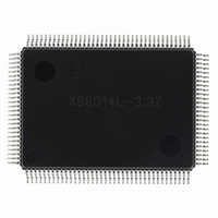
X98014L128-3.3-Z Intersil, X98014L128-3.3-Z Datasheet - Page 12

X98014L128-3.3-Z
Manufacturer Part Number
X98014L128-3.3-Z
Description
IC VIDEO DIGITIZER TRPL 128MQFP
Manufacturer
Intersil
Type
Video Digitizer, 3-Channel AFEr
Datasheet
1.X98014L128-3.3-Z.pdf
(29 pages)
Specifications of X98014L128-3.3-Z
Applications
LCD TV/Monitor
Mounting Type
Surface Mount
Package / Case
128-MQFP, 128-PQFP
Rohs Compliant
Yes
Lead Free Status / RoHS Status
Lead free / RoHS Compliant
Available stocks
Company
Part Number
Manufacturer
Quantity
Price
Company:
Part Number:
X98014L128-3.3-Z
Manufacturer:
Intersil
Quantity:
3
Company:
Part Number:
X98014L128-3.3-Z
Manufacturer:
Intersil
Quantity:
1 900
Part Number:
X98014L128-3.3-Z
Manufacturer:
INTERSIL
Quantity:
20 000
Register Listing
0x05
0x06
0x07
0x08
0x09
0x0A
0x0B
0x0C
ADDRESS
Input configuration (0x00)
Red Gain (0x55)
Green Gain (0x55)
Blue Gain (0x55)
Red Offset (0x80)
Green Offset (0x80)
Blue Offset (0x80)
Offset DAC Configuration (0x00)
REGISTER (DEFAULT VALUE)
(Continued)
12
0
1
2
3
4
5
7:6
7:0
7:0
7:0
7:0
7:0
7:0
0
1
3:2
5:4
7:6
BIT(s)
Channel Select
Input Coupling
RGB/YUV
Sync Type
Composite Sync
Source
COAST CLAMP
enable
Reserved
Red Gain
Green Gain
Blue Gain
Red Offset
Green Offset
Blue Offset
Offset DAC Range
Reserved
Red Offset DAC LSBs These bits are the LSBs necessary for 10 bit manual offset
Green Offset DAC
LSBs
Blue Offset DAC
LSBs
FUNCTION NAME
X98014
0: VGA1
1: VGA2
0: AC coupled (positive input connected to clamp DAC
during clamp time, negative input disconnected from outside
pad and always internally tied to appropriate clamp DAC)
1: DC coupled (+ and - inputs are brought to pads and never
connected to clamp DACs). Analog clamp signal is turned off
in this mode.
0: RGB inputs (Clamp DAC = 300mV for R, G, B, half scale
analog shift for R, G, and B, base ABLC™ target code = 0x00
for R, G, and B)
1: YUV inputs (Clamp DAC = 600mV for R and B, 300mV for
G, half scale analog shift for G channel only, base ABLC™
target code = 0x00 for G, = 0x80 for R and B)
0: Separate HSYNC/VSYNC
1: Composite (from SOG or CSYNC on HSYNC)
0: SOG
1: HSYNC
Note: If Sync Type = 0, the multiplexer will pass HSYNC
regardless of the state of this bit.
0: DC restore clamping and ABLC™ suspended during
COAST
1: DC restore clamping and ABLC™ continue during COAST
Set to 00.
Channel gain, where:
gain (V/V) = 0.5 + [7:0]/170
0x00: gain = 0.5 V/V
(1.4VP-P input = full range of ADC)
0x55: gain = 1.0 V/V
(0.7VP-P input = full range of ADC)
0xFF: gain = 2.0 V/V
(0.35VP-P input = full range of ADC)
ABLC™ enabled: digital offset control. A 1 LSB change in
this register will shift the ADC output by 1 LSB.
ABLC™ disabled: analog offset control. These bits go to the
upper 8 bits of the 10 bit offset DAC. A 1LSB change in this
register will shift the ADC output approximately 1 LSB (Offset
DAC range = 0) or 0.5LSBs (Offset DAC range = 1).
0x00 = min DAC value or -0x80 digital offset,
0x80 = mid DAC value or 0x00 digital offset,
0xFF = max DAC value or +0x7F digital offset
0: ±1/2 ADC fullscale (1 DAC LSB ~ 1 ADC LSB)
1: ±1/4 ADC fullscale (1 DAC LSB ~ 1/2 ADC LSB)
Set to 0.
DAC control.
Combine with their respective MSBs in registers 0x09, 0x0A,
and 0x0B to achieve 10 bit offset DAC control.
IN
IN
DESCRIPTION
March 8, 2006
FN8217.3
IN


