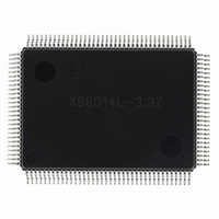
X98014L128-3.3-Z Intersil, X98014L128-3.3-Z Datasheet - Page 18

X98014L128-3.3-Z
Manufacturer Part Number
X98014L128-3.3-Z
Description
IC VIDEO DIGITIZER TRPL 128MQFP
Manufacturer
Intersil
Type
Video Digitizer, 3-Channel AFEr
Datasheet
1.X98014L128-3.3-Z.pdf
(29 pages)
Specifications of X98014L128-3.3-Z
Applications
LCD TV/Monitor
Mounting Type
Surface Mount
Package / Case
128-MQFP, 128-PQFP
Rohs Compliant
Yes
Lead Free Status / RoHS Status
Lead free / RoHS Compliant
Available stocks
Company
Part Number
Manufacturer
Quantity
Price
Company:
Part Number:
X98014L128-3.3-Z
Manufacturer:
Intersil
Quantity:
3
Company:
Part Number:
X98014L128-3.3-Z
Manufacturer:
Intersil
Quantity:
1 900
Part Number:
X98014L128-3.3-Z
Manufacturer:
INTERSIL
Quantity:
20 000
SYNC Processing
The X98014 can process sync signals from 3 different
sources: discrete HSYNC and VSYNC, composite sync on
the HSYNC input, or composite sync from a Sync-On-Green
(SOG) signal embedded on the Green video input. The
X98014 has SYNC activity detect functions to help the
firmware determine which sync source is available.
PGA
The X98014’s Programmable Gain Amplifier (PGA) has a
nominal gain range from 0.5V/V (-6dB) to 2.0V/V (+6dB).
The transfer function is:
where GainCode is the value in the Gain register for that
particular color. Note that for a gain of 1 V/V for GainCode
should be 85 (0x55). This is a different center value than the
128 (0x80) value used by some other AFEs, so the firmware
should take this into account when adjusting gains.
Gain
CLOCKINV
HSYNC
VSYNC
HSYNC
VSYNC
XTAL
SOG
SOG
XTAL
V
--- -
V
OUT
IN
IN
IN
IN
IN
IN
IN
IN
1
1
1
2
2
2
=
0.5
+
GainCode
---------------------------- -
HSYNC2
0x03[6:4]
HSYNC1
0x03[2:0]
SLICER
SLICER
SLICER
SLICER
SOG
0x1C
SOG
0x1C
170
18
POLARITY 0x02[5:0]
ACTIVITY 0x01[6:0]
÷2
DETECT
&
0: ÷1
0x13
1: ÷2
[6]
0x05[0]
VGA1
VGA2
0:
1:
FIGURE 8. SYNC FLOW
HSYNC
SOG
VSYNC
0x11, 0x12, 0x13[2]
GENERATION
0x0E through 0x13
IN
X98014
COAST
IN
IN
PLL
SOURCE
HSYNC
0x05[4:3]
CSYNC
00, 10,
SOG
11:
01:
IN
IN
The PGAs are updated by the internal clamp signal once per
line. In normal operation this means that there is a maximum
delay of one HSYNC period between a write to a Gain
register for a particular color and the corresponding change
in that channel’s actual PGA gain. If there is no regular
HSYNC/SOG source, or if the external clamp option is
enabled (register 0x13[5:4]) but there is no external clamp
signal being generated, it may take up to 100ms for a write
to the Gain register to update the PGA. This is not an issue
in normal operation with RGB and YUV signals.
Bandwidth and Peaking Control
Register 0x0D[3:1] controls a low pass filter allowing the
input bandwidth to be adjusted with three bit resolution
between its default value (0x0E = 780MHz) and its minimum
bandwidth (0x00, for 100MHz). Typically the higher the
resolution, the higher the desired input bandwidth. To
minimize noise, video signals should be digitized with the
minimum bandwidth setting that passes sharp edges.
Pixel Data
from AFE
HS
PIXCLK
SPLITTER
SYNC
24
VSYNC
VSYNC
SYNC
SPLTR
0x05[3]
TYPE
SYNC
Formatter
1:
0:
Output
0x18,
0x19,
0x1A
IN
XTALCLOCK
VSYNC
HSYNC
DATACLK
DATACLK
March 8, 2006
R
R
G
G
B
B
HS
VS
P
S
P
S
P
S
[7:0]
[7:0]
[7:0]
[7:0]
[7:0]
[7:0]
FN8217.3
OUT
OUT
OUT
OUT
OUT


