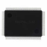
X98014L128-3.3-Z Intersil, X98014L128-3.3-Z Datasheet - Page 25

X98014L128-3.3-Z
Manufacturer Part Number
X98014L128-3.3-Z
Description
IC VIDEO DIGITIZER TRPL 128MQFP
Manufacturer
Intersil
Type
Video Digitizer, 3-Channel AFEr
Datasheet
1.X98014L128-3.3-Z.pdf
(29 pages)
Specifications of X98014L128-3.3-Z
Applications
LCD TV/Monitor
Mounting Type
Surface Mount
Package / Case
128-MQFP, 128-PQFP
Rohs Compliant
Yes
Lead Free Status / RoHS Status
Lead free / RoHS Compliant
Available stocks
Company
Part Number
Manufacturer
Quantity
Price
Company:
Part Number:
X98014L128-3.3-Z
Manufacturer:
Intersil
Quantity:
3
Company:
Part Number:
X98014L128-3.3-Z
Manufacturer:
Intersil
Quantity:
1 900
Part Number:
X98014L128-3.3-Z
Manufacturer:
INTERSIL
Quantity:
20 000
This is a rarely used composite sync format; in most
applications it will never be encountered. However if this
CSYNC waveform must be supported, there is a simple
applications solution using an XOR gate.
The output of the XOR gate is connected to the HSYNC
input of the X98014. One of the XOR inputs is connected to
the HSYNC/CSYNC source, and the other input is
connected to a general purpose I/O. For all sync sources
except the CSYNC shown in Figure 11, the input connected
to the GPIO should be driven low.
If the system microcontroller detects a mode corresponding
to the sync type and polarity shown in Figure 11, it should
drive the GPIO pin high. This will invert the CSYNC signal
seen by the X98014 and prevent any spontaneous image
shifting.
X98014 Serial Communication
Overview
The X98014 uses a 2 wire serial bus for communication with
its host. SCL is the Serial Clock line, driven by the host, and
SDA is the Serial Data line, which can be driven by all
devices on the bus. SDA is open drain to allow multiple
devices to share the same bus simultaneously.
Communication is accomplished in three steps:
The X98014 has a 7 bit address on the serial bus. The upper
6 bits are permanently set to 100110, with the lower bit
determined by the state of pin 48. This allows 2 X98014s to
be independently controlled while sharing the same bus.
1. The Host selects the X98014 it wishes to communicate
2. The Host writes the initial X98014 Configuration Register
3. The Host writes to or reads from the X98014’s
HSYNC
with.
address it wishes to write to or read from.
Configuration Register. The X98014’s internal address
pointer auto increments, so to read registers 0x00
through 0x1B, for example, one would write 0x00 in step
2, then repeat step 3 28 times, with each read returning
the next register value.
IN
Conditions required: negative polarity VSYNC, with no serrations, and t
FIGURE 11. CSYNC ON HSYNC THAT MAY CAUSE SPORADIC IMAGE SHIFTS
25
t
1
IN
X98014
The bus is nominally inactive, with SDA and SCL high.
Communication begins when the host issues a START
command by taking SDA low while SCL is high (Figure 12).
The X98014 continuously monitors the SDA and SCL lines
for the start condition and will not respond to any command
until this condition has been met. The host then transmits the
7 bit serial address plus a R/W bit, indicating if the next
transaction will be a Read (R/W = 1) or a Write (R/W = 0). If
the address transmitted matches that of any device on the
bus, that device must respond with an ACKNOWLEDGE
(Figure 13).
Once the serial address has been transmitted and
acknowledged, one or more bytes of information can be
written to or read from the slave. Communication with the
selected device in the selected direction (read or write) is
ended by a STOP command, where SDA rises while SCL is
high (Figure 12), or a second START command, which is
commonly used to reverse data direction without
relinquishing the bus.
Data on the serial bus must be valid for the entire time SCL
is high (Figure 14). To achieve this, data being written to the
X98014 is latched on a delayed version of the rising edge of
SCL. SCL is delayed and deglitched inside the X98014 for 3
crystal clock periods (120ns for a 25MHz crystal) to eliminate
spurious clock pulses that could disrupt serial
communication.
When the contents of the X98014 are being read, the SDA
line is updated after the falling edge of SCL, delayed and
deglitched in the same manner.
Configuration Register Write
Figure 15 shows two views of the steps necessary to write
one or more words to the Configuration Register.
Configuration Register Read
Figure 16 shows two views of the steps necessary to read
one or more words from the Configuration Register.
1
= t
t
2
2
March 8, 2006
FN8217.3


