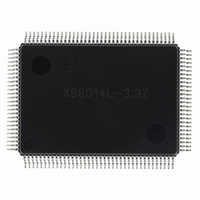
X98014L128-3.3-Z Intersil, X98014L128-3.3-Z Datasheet - Page 20

X98014L128-3.3-Z
Manufacturer Part Number
X98014L128-3.3-Z
Description
IC VIDEO DIGITIZER TRPL 128MQFP
Manufacturer
Intersil
Type
Video Digitizer, 3-Channel AFEr
Datasheet
1.X98014L128-3.3-Z.pdf
(29 pages)
Specifications of X98014L128-3.3-Z
Applications
LCD TV/Monitor
Mounting Type
Surface Mount
Package / Case
128-MQFP, 128-PQFP
Rohs Compliant
Yes
Lead Free Status / RoHS Status
Lead free / RoHS Compliant
Available stocks
Company
Part Number
Manufacturer
Quantity
Price
Company:
Part Number:
X98014L128-3.3-Z
Manufacturer:
Intersil
Quantity:
3
Company:
Part Number:
X98014L128-3.3-Z
Manufacturer:
Intersil
Quantity:
1 900
Part Number:
X98014L128-3.3-Z
Manufacturer:
INTERSIL
Quantity:
20 000
Clock Generation
A Digital Phase Lock Loop (DPLL) is employed to generate
the pixel clock frequency. The HSYNC input and the external
XTAL provide a reference frequency to the PLL. The PLL
then generates the pixel clock frequency that is equal to the
incoming HSYNC frequency times the HTOTAL value
programmed into registers 0x0E and 0x0F.
The stability of the clock is very important and correlates
directly with the quality of the image. During each pixel time
transition, there is a small window where the signal is
slewing from the old pixel amplitude and settling to the new
pixel value. At higher frequencies, the pixel time transitions
at a faster rate, which makes the stable pixel time even
smaller. Any jitter in the pixel clock reduces the effective
stable pixel time and thus the sample window in which pixel
sampling can be made accurately.
Sampling Phase
The X98014 provides 64 low-jitter phase choices per pixel
period, allowing the firmware to precisely select the optimum
sampling point. The sampling phase register is 0x10.
HSYNC Slicer
To further minimize jitter, the HSYNC inputs are treated as
analog signals, and brought into a precision slicer block with
thresholds programmable in 400mV steps with 240mV of
hysteresis, and a subsequent digital glitch filter that ignores
any HSYNC transitions within 100ns of the initial transition.
This processing greatly increases the AFE’s rejection of
ringing and reflections on the HSYNC line and allows the
AFE to perform well even with pathological HSYNC signals.
Voltages given above and in the HSYNC Slicer register
description are with respect to a 3.3V sync signal at the
HSYNC
series resistor should be placed between the HSYNC source
and the HSYNC
hysteresis will be 240mV*5V/3.3V = 360mV, and the slicer
step size will be 400mV*5V/3.3V = 600mV per step.
The best HSYNC slicer threshold is generally 800mV (001b)
when locking on the rising edge of an HSYNC signal, or 2.4V
(110b) when locking on the falling edge.
OFFSET DAC
RANGE
0x0C[0]
IN
0
1
0
1
input pin. To achieve 5V compatibility, a 680Ω
IN
input pin. Relative to a 5V input, the
0.125 ADC LSBs
0.125 ADC LSBs
0.25 ADC LSBs
0.25 ADC LSBs
RESOLUTION
OFFSET DAC
(0.68mV)
(0.34mV)
(0.68mV)
(0.34mV)
10 BIT
20
TABLE 5. OFFSET DAC RANGE AND OFFSET DAC ADJUSTMENT
(ABLC on)
(ABLC on)
(ABLC off)
(ABLC off)
ABLC™
0x17[0]
0
0
1
1
RESOLUTION USING REGISTERS
X98014
(8 BIT OFFSET CONTROL)
USER OFFSET CONTROL
(analog offset control)
(analog offset control)
(digital offset control)
(digital offset control)
0x09 - 0x0B ONLY
1.0 ADC LSB
0.5 ADC LSB
1 ADC LSB
1 ADC LSB
SOG Slicer
The SOG input has programmable threshold, 40mV of
hysteresis, and an optional low pass filter than can be used
to remove high frequency video spikes (generated by
overzealous video peaking in a DVD player, for example)
that can cause false SOG triggers. The SOG threshold sets
the comparator threshold relative to the sync tip (the bottom
of the SOG pulse). A good default SOG slicer threshold
setting is 0x16 (hysteresis and low pass filter enabled,
threshold lowered slightly to accommodate weak sync tips).
SYNC Status and Polarity Detection
The SYNC Status register (0x01) and the SYNC Polarity
register (0x02) continuously monitor all 6 sync inputs
(VSYNC
and report their status. However, accurate sync activity
detection is always a challenge. Noise and repetitive video
patterns on the Green channel may look like SOG activity
when there actually is no SOG signal, while non-standard
SOG signals and trilevel sync signals may have amplitudes
below the default SOG slicer levels and not be easily
detected. As a consequence, not all of the activity detect bits
in the X980xx are correct under all conditions.
Table 6 shows how to use the SYNC Status register (0x01)
to identify the presence of and type of a sync source. The
firmware should go through the table in the order shown,
stopping at the first entry that matches the activity indicators
in the SYNC Status register.
Final validation of composite sync sources (SOG or
Composite sync on HSYNC) should be done by setting the
Input Configuration register (0x05) to the composite sync
source determined by this table, and confirming that the
CSYNC detect bit is set.
The accuracy of the Trilevel Sync detect bit can be increased
by multiple reads of the Trilevel Sync detect bit. See the
Trilevel Sync Detect section for more details.
For best SOG operation, the SOG low pass filter (register
0x04[4]) should always be enabled to reject the high
frequency peaking often seen on video signals.
IN
, HSYNC
IN
, and SOG
RESOLUTION USING REGISTERS
(10 BIT OFFSET CONTROL)
0x09 - 0x0B AND 0x0C[7:2]
USER OFFSET CONTROL
(analog offset control)
(analog offset control)
IN
0.125 ADC LSB
0.25 ADC LSB
for each of 2 channels)
N/A
N/A
March 8, 2006
FN8217.3


