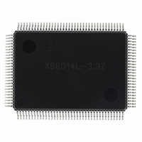
X98014L128-3.3-Z Intersil, X98014L128-3.3-Z Datasheet - Page 13

X98014L128-3.3-Z
Manufacturer Part Number
X98014L128-3.3-Z
Description
IC VIDEO DIGITIZER TRPL 128MQFP
Manufacturer
Intersil
Type
Video Digitizer, 3-Channel AFEr
Datasheet
1.X98014L128-3.3-Z.pdf
(29 pages)
Specifications of X98014L128-3.3-Z
Applications
LCD TV/Monitor
Mounting Type
Surface Mount
Package / Case
128-MQFP, 128-PQFP
Rohs Compliant
Yes
Lead Free Status / RoHS Status
Lead free / RoHS Compliant
Available stocks
Company
Part Number
Manufacturer
Quantity
Price
Company:
Part Number:
X98014L128-3.3-Z
Manufacturer:
Intersil
Quantity:
3
Company:
Part Number:
X98014L128-3.3-Z
Manufacturer:
Intersil
Quantity:
1 900
Part Number:
X98014L128-3.3-Z
Manufacturer:
INTERSIL
Quantity:
20 000
Register Listing
0x0D
0x0E
0x0F
0x10
0x11
0x12
0x13
0x14
0x15
0x16
ADDRESS
AFE Bandwidth (0x0E)
PLL Htotal MSB (0x03)
PLL Htotal LSB (0x20)
PLL Sampling Phase (0x00)
PLL Pre-coast (0x08)
PLL Post-coast (0x00)
PLL Misc (0x00)
DC Restore and ABLC™ starting
pixel MSB (0x00)
DC Restore and ABLC™ starting
pixel LSB (0x00)
DC Restore Clamp Width
(0x10)
REGISTER (DEFAULT VALUE)
(Continued)
13
0
3:1
7:4
5:0
7:0
5:0
7:0
7:0
0
1
2
3
5:4
6
7
4:0
7:0
7:0
BIT(s)
Unused
AFE BW
Peaking
PLL Htotal MSB
PLL Htotal LSB
PLL Sampling Phase
Pre-coast
Post-coast
PLL Lock Edge
HSYNC1
PLL Lock Edge
HSYNC2
Reserved
CLKINV
Disable
CLKINV
Function
XTALCLKOUT
Frequency
Disable
XTALCLKOUT
DC Restore and
ABLC™ starting
pixel (MSB)
DC Restore and
ABLC™ starting
pixel (LSB)
DC Restore clamp
width (pixels)
FUNCTION NAME
X98014
IN
IN
Pin
Pin
Value doesn’t matter
3dB point for AFE lowpass filter
000: 100MHz
111: 780MHz (default)
0000: Disabled (default) See Bandwidth and Peaking
Control section for more information
14 bit HTOTAL (number of active pixels) value
The minimum HTOTAL value supported is 0x200.
HTOTAL to PLL is updated on LSB write only.
Used to control the phase of the ADC’s sample point relative
to the period of a pixel. Adjust to obtain optimum image
quality. One step = 5.625° (1.56% of pixel period).
Number of lines the PLL will coast prior to the start of
VSYNC. Applies only to internally generated COAST
signals.
Number of lines the PLL will coast after the end of VSYNC.
Applies only to internally generated COAST signals.
0: Lock on trailing edge of HSYNC1 (default)
1: Lock on leading edge of HSYNC1
0: Lock on trailing edge of HSYNC2 (default)
1: Lock on leading edge of HSYNC2
Set to 0.
0: CLKINV
1: CLKINV
00: CLKINV (default)
01: External CLAMP (see Note)
10: External COAST
11: External PIXCLK
Note: the CLAMP pulse is used to
- perform a DC restore (if enabled)
- start the ABLC™ function (if enabled), and
- update the data to the Offset DACs (always).
When in the default internal CLAMP mode, the X98014
automatically generates the CLAMP pulse. If External
CLAMP is selected, the Offset DAC values will only change
on the leading edge of CLAMP. If there is no internal clamp
signal, there will be up to a 100ms delay between when the
PGA gain or offset DAC register is written to, and when the
PGA or offset DAC is actually updated.
0: XTALCLK
1: XTALCLK
0 = XTALCLK
1 = XTALCLK
Pixel after HSYNC
DC restore and ABLC™ functions. 13 bits.
Set this register to the first stable black pixel following the
trailing edge of HSYNC
Width of DC restore clamp used in AC-coupled
configurations. Has no effect on ABLC™. Minimum value is
0x02 (a setting of 0x01 or 0x00 will not generate a clamp
pulse).
IN
IN
OUT
OUT
pin enabled (default)
pin disabled (internally forced low)
OUT
OUT
= f
= f
enabled
is logic low
IN
CRYSTAL
CRYSTAL
trailing edge to begin
DESCRIPTION
IN
.
/2
(default)
March 8, 2006
FN8217.3


