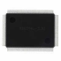
X98014L128-3.3-Z Intersil, X98014L128-3.3-Z Datasheet - Page 23

X98014L128-3.3-Z
Manufacturer Part Number
X98014L128-3.3-Z
Description
IC VIDEO DIGITIZER TRPL 128MQFP
Manufacturer
Intersil
Type
Video Digitizer, 3-Channel AFEr
Datasheet
1.X98014L128-3.3-Z.pdf
(29 pages)
Specifications of X98014L128-3.3-Z
Applications
LCD TV/Monitor
Mounting Type
Surface Mount
Package / Case
128-MQFP, 128-PQFP
Rohs Compliant
Yes
Lead Free Status / RoHS Status
Lead free / RoHS Compliant
Available stocks
Company
Part Number
Manufacturer
Quantity
Price
Company:
Part Number:
X98014L128-3.3-Z
Manufacturer:
Intersil
Quantity:
3
Company:
Part Number:
X98014L128-3.3-Z
Manufacturer:
Intersil
Quantity:
1 900
Part Number:
X98014L128-3.3-Z
Manufacturer:
INTERSIL
Quantity:
20 000
Crystal Oscillator
An external 23MHz to 27MHz crystal supplies the low-jitter
reference clock to the DPLL. The absolute frequency of this
crystal within this range is unimportant, as is the crystal’s
temperature coefficient, allowing use of less expensive,
lower-grade crystals.
EMI Considerations
There are two possible sources of EMI on the X98014:
• Crystal oscillator. The EMI from the crystal oscillator is
• Digital output switching. This is the largest potential
Recommendations for minimizing EMI are:
• Minimize the databus trace length
• Minimize the databus capacitive loading.
Analog Video In
negligible. This is due to an amplitude-regulated, low
voltage sine wave oscillator circuit, instead of the typical
high-gain square wave inverter-type oscillator, so there
are no harmonics. The crystal oscillator is not a significant
source of EMI.
source of EMI. However, the EMI is determined by the
PCB+ layout and the loading on the databus. The way to
control this is to put series resistors on the output of all the
digital pins. These resistor values should be adjusted to
optimize signal quality on the bus. Intersil recommends
starting with 22Ω and adjusting as necessary for the
particular PCB layout and device loading.
DATACLK (A)
DATACLK (B)
(to A and B)
(to A and B)
HS
HS
DATA (A)
DATA (B)
HSYNC
OUT
OUT
(A)
(B)
IN
P
N-3
P
N-2
23
P
N-1
P
N
DPLL Lock Edge
FIGURE 9. ALTERNATE PIXEL SAMPLING (24 BIT MODE)
P
0
P
CLKINV
1
P
CLKINV
2
P
IN
3
(A) = GND
P
IN
4
(B) = V
P
5
X98014
P
6
D
D
P
7
If EMI is a problem in the final design, increase the value of
the digital output series resistors to reduce slew rates on the
bus. This can only be done as long as the scaler’s setup and
hold timing requirements continue to be met.
Alternate Pixel Sampling
Two X98014s (AFE
simultaneously to achieve effective sample rates greater
than 140MHz. Each AFE is programmed with an HTOTAL
value equal to one-half of the total number of pixels in a line.
The CLOCKINV
tied to V
though some minor phase adjustment may be needed to
compensate for any propagation delay mismatch between
the two AFEs.
The CLOCKINV
degrees from AFE
the rising edge of its DATACLK, while AFE
pixels on the rising edge of its clock. With each AFE in 24 bit
mode, two 24 bit data streams are generated (Figure 9).
With both AFEs configured for 48 bit mode, a 96 bit
datastream is generated (Figure 10).
In both cases, AFE
domains. In 24 bit mode, the data from each AFE must be
latched on the rising edge of that AFE’s DATACLK. In 48 bit
mode, the frequencies are low enough that the rising edge of
AFE B can be used to capture both AFE
P
8
P
9
D
P
. Both AFEs are otherwise programmed identically,
10
P
11
IN
IN
P
A
pin for AFE
setting shifts the phase of AFE
12
A
½ DATACLK Delay
A
. AFE
and AFE
and AFE
A
D
now samples the even pixels on
N-3
B
A
D
B
) may be used
N-2
are on different DATACLK
is tied to ground, AFE
D
N-1
D
B
N
B
and AFE
D
samples the odd
0
D
1
B
March 8, 2006
A
by 180
D
data.
2
FN8217.3
B
D
3
is


