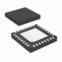
LMH1982SQE/NOPB National Semiconductor, LMH1982SQE/NOPB Datasheet - Page 13

LMH1982SQE/NOPB
Manufacturer Part Number
LMH1982SQE/NOPB
Description
IC CLK GEN MULTI RATE VID 32-LLP
Manufacturer
National Semiconductor
Type
Clock Generatorr
Datasheet
1.LMH1982SQENOPB.pdf
(34 pages)
Specifications of LMH1982SQE/NOPB
Applications
Displays, Projectors, Receivers
Mounting Type
Surface Mount
Package / Case
32-LLP
For Use With
LMH1982SQEEVAL - BOARD EVAL FOR LMH1982SQE
Lead Free Status / RoHS Status
Lead free / RoHS Compliant
Other names
LMH1982SQETR
1. The PLL 1 reference divider value is not the same as the programming value for REF_DIV_SEL. See Table 3.
Application Information
1.0 FUNCTIONAL OVERVIEW
The LMH1982 is an analog phase locked loop (PLL) clock
generator that can output simultaneous SD and HD video
clocks synchronized or “genlocked” to H sync and V sync in-
put reference timing. The LMH1982 features an output Top of
Frame (TOF) pulse generator with programmable timing that
can also be synchronized to the reference frame. Two refer-
ence ports are provided to allow a secondary input to be
selected.
The clock generator uses a two-stage PLL architecture. The
first stage is a VCXO-based PLL (PLL 1) that requires an ex-
ternal 27 MHz VCXO and loop filter. In Genlock mode, PLL 1
can phase lock the VCXO clock to the input reference after
programming the PLL divider ratio. The use of a VCXO pro-
vides a low phase noise clock source even when the
LMH1982 is configured with a low loop bandwidth, which is
necessary to attenuate input timing jitter for minimum jitter
transfer. The combination of the external VCXO, external loop
filter, and programmable PLL parameters can provide flexi-
bility for the system designer to optimize the loop bandwidth
and loop response for the application.
The second stage consists of three PLLs (PLL 2, 3, 4) with
integrated VCOs and loop filters. These PLLs will attempt to
continually track the reference VCXO clock phase from
PLL 1 regardless of the device mode. The second stage PLLs
have pre-configured divider ratios to provide frequency mul-
tiplication or translation from the VCXO clock frequency. The
2.0 GENERAL INFORMATION
For normal operation, the RESET pin must be set high; oth-
erwise, the device cannot be programmed and will not func-
tion properly. To reset the control registers to their default
values, toggle RESET low for at least 10 µs and then set high.
sample clock
48 kHz AES
1080i/59.94
1080i/60
1080i/50
PLL 1
PLL 2
PLL 3
PLL 4
Format
PLL
Input Reference
Reference
Divider
PLL 1
VCXO clock
VCXO clock
VCXO clock
[5]
[5]
1
5
1
2
H sync
1
INPUT TIMING PARAMETERS
Feedback
Divider
PLL 1
[4000]
[4800]
4004
1125
800
960
(Note 20)
TABLE 2. LMH1982 PLL and Clock Summary
Divider Ratio (reduced)
PLL 1 Phase
Comparison
Frequency
250/91 or 500/91
Programmable
6.7433
28.125
[5.625]
11/4 or 11/2
33.75
[6.75]
(kHz)
24.0
5/2
Total Lines
per Frame
Counter
13
1125
[225]
1125
1125
[225]
96
VCO PLLs use a high loop bandwidth to assure PLL stability,
so the VCXO must provide a stable low-jitter clock reference
to ensure optimal output jitter performance.
Any unused clock output can be put in Hi-Z mode, which can
be useful for reducing power dissipation as well as reducing
jitter or phase noise on the active clock output.
The TOF pulse can be programmed to indicate the start (top)
of frame and even provide format cross-locking. The output
format registers should be programmed to specify the output
timing (output clocks and TOF pulse), the output timing offset
relative to the reference, and the output initialization (align-
ment) to the reference frame. If unused, the TOF output can
also be put in Hi-Z mode.
When a loss of reference occurs during genlock, PLL 1 can
default to either Free run or Holdover operation. When free
run is selected, the output frequency accuracy will be deter-
mined by the external bias on the free run control voltage input
pin, VC_FREERUN. When Holdover is selected, the loop filter
can hold the control voltage to maintain short-term output
phase accuracy for a brief period in order to allow the appli-
cation to select the secondary input reference and re-lock the
outputs. These options in combination with proper PLL 1 loop
response design can provide flexibility to manage output
clock behavior during loss and re-acquisition of the reference.
The reference status and PLL lock status flags can provide
real-time status indication to the application system. The loss
of reference and lock detection thresholds can also be con-
figured.
The LMH1982 can be configured by programming the control
registers via the I
DCh for write sequences and DDh for read sequences. The
I
communication; otherwise, the LMH1982 will not acknowl-
edge read/write sequences.
2
C_ENABLE pin must be set low or tied to GND to allow I
Frequency
74.25/1.001 (74.176) or
74.176
148.5/1.001 (148.35)
Clock
(MHz)
(27.0)
(27.0)
(27.0)
74.25
74.25
27.0
Frequency (MHz)
74.25 or 148.5
Output Clock
OUTPUT TIMING PARAMETERS
67.5
2
27
C interface. The I
Total Clocks
per Line
Counter
(4004)
(800)
(960)
2200
2200
2640
1125
(Note 21)
Total Lines
per Frame
Counter
2
C slave addresses are
(1125)
(1125)
(225)
1125
1125
1125
96
Output Port
SD_CLK
HD_CLK
HD_CLK
SD_CLK
www.national.com
Frame
29.97
Rate
(Hz)
250
30
25
2
C


