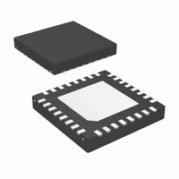
LMH1982SQE/NOPB National Semiconductor, LMH1982SQE/NOPB Datasheet - Page 19

LMH1982SQE/NOPB
Manufacturer Part Number
LMH1982SQE/NOPB
Description
IC CLK GEN MULTI RATE VID 32-LLP
Manufacturer
National Semiconductor
Type
Clock Generatorr
Datasheet
1.LMH1982SQENOPB.pdf
(34 pages)
Specifications of LMH1982SQE/NOPB
Applications
Displays, Projectors, Receivers
Mounting Type
Surface Mount
Package / Case
32-LLP
For Use With
LMH1982SQEEVAL - BOARD EVAL FOR LMH1982SQE
Lead Free Status / RoHS Status
Lead free / RoHS Compliant
Other names
LMH1982SQETR
5.2.1 Output TOF Clock
The TOF pulse is derived from a counter chain, which re-
ceives either output clock (SD_CLK or HD_CLK) from a 2:1
MUX block, as shown in Figure 3. The TOF clock from the
MUX can be selected by programming TOF_CLK (register
0Ch). To select SD_CLK as the TOF clock, set TOF_CLK =
0; otherwise, set TOF_CLK = 1 to select HD_CLK. The se-
lected TOF clock frequency is determined by the SD_FREQ
or HD_FREQ register setting.
The TOF output delay time (t
erated from a TOF clock of 27 MHz is specified in the Elec-
trical Characteristics table. The TOF output delay time for 525i
and 1080i/50 generated using 27 MHz and 74.25 MHz, re-
spectively, are shown in the Typical Performance Character-
istics section. The TOF pulse width can be determined by:
Where:
5.2.2 Output Frame Timing
The TOF pulse is specified by programming TOF_CLK,
TOF_PPL (register 0Bh-0Ch) and TOF_LPFM (register
0Dh-0Eh). These registers configure the 2:1 MUX and output
pixel and line counters in the TOF Generation blocks shown
in Figure 3. The output frame or TOF pulse rate is determined
by:
Where:
Example:
If the output format is 625i, then:
Where:
5.2.2.1 HD Format TOF Generation using a 27 MHz TOF
Clock
Any HD format TOF pulse can be generated using either: Op-
tion 1) its native HD clock frequency, or Option 2) the 27 MHz
SD clock frequency.
Using Option 1 for HD output formats can result in TOF output
delay being offset by more than one TOF clock period, even
after output initialization. This is because the very short period
of the HD native clock yields little timing margin for the reset
signals to propagate through the internal logic in Figure 3. For
example, using a TOF clock of 148.5 MHz gives less than 6.7
ns (< 1 clock cycle) for all the logic to completely synchronize
and guarantee proper output initialization.
To ensure proper output initialization, Option 2 is recom-
mended for HD output formats, especially 1080p at 50, 59.94,
and 60 Hz. This is because the longer period of the 27 MHz
clock provides ample timing margin for the internal logic to
reset. The output parameters for programming the HD output
formats using the 27 MHz clock are shown in Table 1.
TOF pulse width = (1 / f
f
TOF_PPL = Output Format Total Pixels per Line
TOF rate = f
f
TOF_PPL = Output Format Total Pixels per Line
TOF_LPFM = Output Format Total Lines per Frame
TOF rate = 27 MHz / (1728 x 625) = 25 Hz
f
TOF_PPL = 1728
TOF_LPFM = 625
TOF_CLK
TOF_CLK
TOF_CLK
= Nominal TOF Clock Frequency
= Nominal TOF Clock Frequency
= 27 MHz (SD_FREQ = 0)
TOF_CLK
/ (TOF_PPL x TOF_LPFM)
TOF_CLK
D_TOF
) x TOF_PPL
) for any output format gen-
19
To illustrate both TOF clock options, an example is given be-
low for 1080p/59.94, which has a native pixel clock frequency
of 148.5/1.001 MHz and frame rate of 60/1.001 Hz:
Option 1) 1080p/59.94 TOF generation using 148.35 MHz
Where:
Option 2) 1080p/59.94 TOF generation using 27 MHz
Where:
As an example, Figure 4 shows a timing illustration for 1080p/
59 TOF and clock outputs for Option 2. Once the outputs are
initialized, the SD clock and TOF pulse will have a fixed delay,
and the SD clock and HD clock will have a fixed timing offset
relative to each other. Therefore, the timing offset between
the TOF pulse and HD clock, or t
can be determined by:
Where:
5.2.3 Reference Frame Timing
The reference format frame timing is generated internally and
used for resetting the internal counters for output initialization.
The reference frame rate should be specified by programming
the reference format total lines per frame to REF_LPFM (reg-
ister 0Fh-10h) as well as the PLL 1 dividers. See Table 1 for
programming the parameter values according to each refer-
ence format. The reference frame rate is determined by:
Where:
FIGURE 4. Timing Illustration Showing 1080p/59.94 TOF
TOF rate = 148.5/1.001 MHz / (2200 x 1125) = 60/1.001 Hz
f
TOF_PPL = 2200
TOF_LPFM = 1125
TOF rate = 27 MHz / 2002 x 225) = 60/1.001 Hz
f
TOF_PPL = 2002
TOF_LPFM = 225
t
t
t
t
REF rate = (f
f
R_DIV = Reference Divider (not REF_DIV_SEL)
FB_DIV = Feedback Divider
TOF_CLK
TOF_CLK
TOF-HD
D_TOF
D_SD
D_HD
VCXO
= SD_CLK Output Delay Time
= HD_CLK Output Delay Time
= 27 MHz Nominal VCXO Clock Frequency
= TOF Output Delay Time referenced to SD_CLK
and CLK Output Delays Using Option 2
= t
= 148.35 MHz (TOF_CLK = 1, HD_FREQ = 3h)
= 27 MHz (TOF_CLK = 0, SD_FREQ = 0)
D_TOF
VCXO
+ t
x R_DIV) / (FB_DIV x REF_LPFM)
D_SD
- t
D_HD
TOF-HD
, will also be fixed and
www.national.com
30052438


