LMH1982SQE/NOPB National Semiconductor, LMH1982SQE/NOPB Datasheet - Page 5
LMH1982SQE/NOPB
Manufacturer Part Number
LMH1982SQE/NOPB
Description
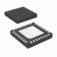
IC CLK GEN MULTI RATE VID 32-LLP
Manufacturer
National Semiconductor
Type
Clock Generatorr
Datasheet
1.LMH1982SQENOPB.pdf
(34 pages)
Specifications of LMH1982SQE/NOPB
Applications
Displays, Projectors, Receivers
Mounting Type
Surface Mount
Package / Case
32-LLP
For Use With
LMH1982SQEEVAL - BOARD EVAL FOR LMH1982SQE
Lead Free Status / RoHS Status
Lead free / RoHS Compliant
Other names
LMH1982SQETR


General Description .............................................................................................................................. 1
Features .............................................................................................................................................. 1
Applications ......................................................................................................................................... 1
Typical Video Genlock Block Diagram ..................................................................................................... 1
Functional Block Diagram ...................................................................................................................... 2
Typical Loop Filter Topology .................................................................................................................. 2
Ordering Information ............................................................................................................................. 2
Connection Diagram ............................................................................................................................. 3
Pin Descriptions ................................................................................................................................... 4
Absolute Maximum Ratings .................................................................................................................... 7
Operating Ratings ................................................................................................................................ 7
Electrical Characteristics ........................................................................................................................ 7
Typical Performance Characteristics ..................................................................................................... 10
Supported Standards and Timing Formats ............................................................................................. 12
Application Information ........................................................................................................................ 13
1.0 FUNCTIONAL OVERVIEW ...................................................................................................... 13
2.0 GENERAL INFORMATION ...................................................................................................... 13
3.0 MODES OF OPERATION ....................................................................................................... 14
4.0 INPUT REFERENCE .............................................................................................................. 15
5.0 OUTPUT CLOCKS AND TOF .................................................................................................. 16
6.0 REFERENCE AND PLL LOCK STATUS ................................................................................... 21
7.0 LOOP RESPONSE ................................................................................................................ 22
8.0 I
9.0 I
2
2
2.1 148.35 MHz PLL Initialization Sequence ............................................................................ 14
2.2 Enabling Genlock Mode ................................................................................................... 14
2.3 Output Disturbance While Output Alignment Mode Enabled .................................................. 14
2.4 Power Supply Sequencing ............................................................................................... 14
2.5 Evaluating the LMH1982 .................................................................................................. 14
3.1 Free Run Mode ............................................................................................................... 14
3.2 Genlock Mode ................................................................................................................ 14
4.1 Programming the PLL 1 Dividers ....................................................................................... 16
4.2 Reference Frame Decoder ............................................................................................... 16
5.1 Programming The Output Clock Frequencies ...................................................................... 16
5.2 Programming The Output Format Timing ............................................................................ 17
5.3 Programming The Output Initialization Sequence ................................................................ 20
5.4 Output Behavior Upon Loss Of Reference .......................................................................... 20
6.1 Reference Detection ........................................................................................................ 21
6.2 PLL Lock Detection ......................................................................................................... 21
TABLE 7. Summary of Genlock Status Bits and Flag Outputs ..................................................... 22
7.1 Loop Response Design Equations ..................................................................................... 22
7.2 Lock Time Considerations ................................................................................................ 23
7.3 VCXO Considerations ...................................................................................................... 23
7.4 Free Run Output Jitter ..................................................................................................... 23
8.1 Write Sequence .............................................................................................................. 23
8.2 Read Sequence .............................................................................................................. 24
8.3 I
C INTERFACE PROTOCOL .................................................................................................. 23
C INTERFACE CONTROL REGISTER DEFINITIONS .............................................................. 25
2
3.2.1 Genlock Mode State Diagram ................................................................................. 15
5.2.1 Output TOF Clock ................................................................................................. 19
5.2.2 Output Frame Timing ............................................................................................. 19
5.2.3 Reference Frame Timing ........................................................................................ 19
5.2.4 Input-Output Frame Rate Ratio ............................................................................... 20
5.2.5 Output Frame Line Offset ....................................................................................... 20
5.3.1 TOF Output Delay Considerations ........................................................................... 20
5.3.2 Output Clock Initialization without TOF ..................................................................... 20
6.1.1 Programming the Loss of Reference (LOR) Threshold ............................................... 21
6.2.1 Programming the PLL Lock Threshold ..................................................................... 21
6.2.2 PLL Lock Status Instability ...................................................................................... 21
7.1.1 Loop Response Optimization Tips ........................................................................... 23
7.1.2 Loop Filter Capacitors ............................................................................................ 23
C Enable Control Pin .................................................................................................... 24
3.2.2 Loss of Reference (LOR) ................................................................................ 15
5.2.2.1 HD Format TOF Generation using a 27 MHz TOF Clock ................................... 19
3.2.2.1 Free Run during LOR ........................................................................... 15
3.2.2.2 Holdover during LOR ............................................................................ 15
Table of Contents
5
www.national.com
Related parts for LMH1982SQE/NOPB
Image
Part Number
Description
Manufacturer
Datasheet
Request
R

Part Number:
Description:
IC CLK GEN MULTI RATE VID 32-LLP
Manufacturer:
National Semiconductor
Datasheet:

Part Number:
Description:
Manufacturer:
National Semiconductor Corporation
Datasheet:

Part Number:
Description:
National Semiconductor [8-Bit D/A Converter]
Manufacturer:
National Semiconductor
Datasheet:
Part Number:
Description:
National Semiconductor [Media Coprocessor]
Manufacturer:
National Semiconductor
Datasheet:
Part Number:
Description:
Digitally Controlled Tone and Volume Circuit with Stereo Audio Power Amplifier, Microphone Preamp Stage and National 3D Sound
Manufacturer:
National Semiconductor
Datasheet:
Part Number:
Description:
Digitally Controlled Tone and Volume Circuit with Stereo Audio Power Amplifier, Microphone Preamp Stage and National 3D Sound
Manufacturer:
National Semiconductor
Datasheet:
Part Number:
Description:
AC97 Rev 2 Codec with Sample Rate Conversion and National 3D Sound
Manufacturer:
National Semiconductor
Part Number:
Description:
Manufacturer:
National Semiconductor
Datasheet:
Part Number:
Description:
Manufacturer:
National Semiconductor
Datasheet:
Part Number:
Description:
General Purpose, Low Voltage, Low Power, Rail-to-Rail Output Operational Amplifiers
Manufacturer:
National Semiconductor
Datasheet:
Part Number:
Description:
8-bit 20 MSPS flash A/D converter.
Manufacturer:
National Semiconductor
Datasheet:
Part Number:
Description:
Low Noise Quad Operational Amplifier
Manufacturer:
National Semiconductor
Datasheet:
Part Number:
Description:
Quad Differential Line Receivers
Manufacturer:
National Semiconductor
Datasheet:
Part Number:
Description:
Quad High Speed Trapezoidal? Bus Transceiver
Manufacturer:
National Semiconductor
Datasheet: