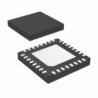
LMH1982SQE/NOPB National Semiconductor, LMH1982SQE/NOPB Datasheet - Page 22

LMH1982SQE/NOPB
Manufacturer Part Number
LMH1982SQE/NOPB
Description
IC CLK GEN MULTI RATE VID 32-LLP
Manufacturer
National Semiconductor
Type
Clock Generatorr
Datasheet
1.LMH1982SQENOPB.pdf
(34 pages)
Specifications of LMH1982SQE/NOPB
Applications
Displays, Projectors, Receivers
Mounting Type
Surface Mount
Package / Case
32-LLP
For Use With
LMH1982SQEEVAL - BOARD EVAL FOR LMH1982SQE
Lead Free Status / RoHS Status
Lead free / RoHS Compliant
Other names
LMH1982SQETR
www.national.com
Status flag output logic equations:
1. NO_REF = REF_VALID
2. NO_LOCK = (REF_VALID) (SD_LOCK) (HD_LOCK)
7.0 LOOP RESPONSE
The overall loop response of the LMH1982 is determined by
the design of the VCXO PLL (PLL 1). Because the integrated
VCO PLLs use the VCXO clock as the input reference to
phase lock the output clocks, the ability of PLL 1 to attenuate
the input jitter is critical to output jitter performance, especially
low-frequency jitter that occurs at the video line and field
rates. The loop response of the LMH1982 can be character-
ized by PLL 1's loop bandwidth and damping factor.
The loop response is primarily determined by the loop filter
components and the loop gain. A passive second-order loop
filter consisting of R
sufficient input jitter attenuation for most applications, al-
though a higher order passive filter or active filter may also be
used. The loop gain is a function of the VCXO gain and pro-
grammable PLL parameters.
A lower loop bandwidth will provide higher input jitter attenu-
ation (reduced jitter transfer) for improved output jitter perfor-
mance; however, increased lock time (or settling time) and
larger external component values are a couple trade-offs to a
lower loop bandwidth.
7.1 Loop Response Design Equations
The following equations can be used to design the loop re-
sponse of PLL 1.
The -3 dB loop bandwidth, BW, can be approximated by:
Where:
I
R
K
Genlock mode, Reference
valid, PLLs locking
Genlock mode, Reference
valid, PLLs locked
Genlock mode, Reference
lost, Free Run operation
Genlock mode, Reference
lost, Holdover operation
CP1
VCO
BW = I
S
=
=
=
CP1
Conditions
Nominal VCXO PLL charge pump current (in
amps)
programmed by setting ICP1 (register 13h).
For example:
I
I
I
I
I
Nominal value of series resistor (in ohms)
Nominal 27 MHz VCXO gain (in Hz/V)
K
CP1
CP1
CP1
CP1
CP1
* R
VCO
S
= 250 µA: ICP1 = 08h (default value)
= 0 µA: ICP1 = 00h (min)
= 62.5 µA; ICP1 = 02h (practical min)
= 968.75 µA; ICP1 = 1Fh (max)
step size = 31.25 µA
= Pull_range * 27 MHz/Vin_range
* K
S
VCO
, C
S
/ FB_DIV
, and C
TABLE 7. Summary of Genlock Status Bits and Flag Outputs
P
Mode Control Bits
GNLK
components can provide
Register 00h
1
1
1
1
HOLD-
OVER
X
X
0
1
NO_REF
(pin 16)
Status Flag Outputs
0
0
1
1
22
1
Note that this BW approximation does not take into account
the effects of the damping factor or the second pole intro-
duced by Cp.
At frequencies far above the −3 dB loop bandwidth, the
closed-loop frequency response of PLL 1 will roll off at about
−40 dB/decade, which is useful attenuating input jitter at fre-
quencies above the loop bandwidth. Near the −3 dB corner
frequency, the roll-off characteristic will depend on other fac-
tors, such as damping factor and filter order.
To prevent output jitter due to the modulation of the VCXO by
the PLL’s phase comparison frequency:
PLL 1's damping factor, DF, can be approximated by:
Where:
A typical design target for DF is between 0.707 to 1, which
can often yield a good trade-off between reference spur at-
tenuation and lock time. DF is related to the phase margin,
which is a measure of the PLL stability.
A secondary parallel capacitor, C
erence spurs introduced by the PLL which may modulate the
VCXO input voltage and also cause output jitter. The following
relationship should be used to determine C
The PLL loop gain, K, can be calculated as:
Therefore, the BW and DF can be expressed in terms of K:
FB_DIV = Feedback Divider value
BW
DF = (R
C
C
K = I
BW = R
DF = (R
NO_LOCK
S
P
(pin 17)
= Nominal value of the series capacitor (in farads)
= C
≤
CP1
1
0
1
1
(27 MHz / FB_DIV) / 20
S
S
S
S
* K
/ 20
/2) * sqrt (C
/ 2) * sqrt (I
* K
For the recommended VCXO (Mftr: CTS, P/N:
357LB3C027M0000): K
(3.0V- 0.3V) = 1000 Hz/V
For example:
FB_DIV =1716 for NTSC timing
VCO
2
HD_LOCK
/ FB_DIV
bit 2
0
1
1
1
S
CP1
* K)
* C
S
Register 01h
* K
Status Bits
SD_LOCK
P
, is needed to filter the ref-
VCO
bit 1
VCO
0
1
0
0
/ FB_DIV)
= 100 ppm * 27 MHz/
P
:
REF_VALID
bit 0
1
1
0
0


