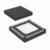
LMH1982SQE/NOPB National Semiconductor, LMH1982SQE/NOPB Datasheet - Page 9

LMH1982SQE/NOPB
Manufacturer Part Number
LMH1982SQE/NOPB
Description
IC CLK GEN MULTI RATE VID 32-LLP
Manufacturer
National Semiconductor
Type
Clock Generatorr
Datasheet
1.LMH1982SQENOPB.pdf
(34 pages)
Specifications of LMH1982SQE/NOPB
Applications
Displays, Projectors, Receivers
Mounting Type
Surface Mount
Package / Case
32-LLP
For Use With
LMH1982SQEEVAL - BOARD EVAL FOR LMH1982SQE
Lead Free Status / RoHS Status
Lead free / RoHS Compliant
Other names
LMH1982SQETR
Note 4: Electrical Table values apply only for factory testing conditions at the temperature indicated. No guarantee of parametric performance is indicated in the
electrical tables under conditions different than those tested.
Note 5: Typical values represent the most likely parametric norm as determined at the time of characterization. Actual typical values may vary over time and will
also depend on the application and configuration. The typical values are not tested and are not guaranteed on shipped production material.
Note 6: Limits are 100% production tested at 25°C. Limits over the operating temperature range are guaranteed through correlation using Statistical Quality
Control (SQC) methods.
Note 7: The input voltage to VC_FREERUN (pin 1) should also be within the input range of the external VCXO. The input voltage should be clean from noise
that may significantly modulate the VCXO control voltage and consequently produce output jitter during free run operation.
Note 8: ΔT
sync timing offset must be within ΔT
ΔT
Note 9: t
Note 10: For any SD and HD output formats, the TOF pulse can be generated using 27 MHz as the TOF clock by programming TOF_CLK = 0, SD_FREQ = 0,
and the alternative output counter values shown in Table 1. See section 5.2.2.1 HD Format TOF Generation using a 27 MHz TOF Clock.
Note 11: Output initialization refers to the initial alignment of the output frame clock and TOF signals to the input reference frame. See section 5.3 Programming
The Output Initialization Sequence.
Note 12: The SD and HD clock output jitter is based on VCXO clock (pin 29) with 20 ps peak-to-peak using a time interval error (TIE) jitter measurement. The
typical TIE peak-to-peak jitter was measured on the LMH1982 evaluation bench board using TDSJIT3 jitter analysis software on a Tektronix DSA70604
oscilloscope and 1 GHz active differential probe.
Note 13: t
taken at the leading edge of the TOF pulse (Note 10), where the input and output clocks are phase aligned at the start of frame.
Note 14: t
taken at the leading edge of the TOF pulse (Note 10), where the input and output clocks are phase aligned at the start of frame.
Note 15: This parameter is specified for the SD_CLK output only. This parameter is guaranteed by design for the HD_CLK output.
TDSJIT3 Clock TIE Measurement Setup: 10
Oscilloscope Setup: 20 mV/div vertical scale, 100 µs/div horizontal scale, and 25 GS/s sampling rate
HV
for all frames. See sections 4.2 Reference Frame Decoder and 5.2.5 Output Frame Line Offset.
D_TOF
D_SD
D_HD
HV
is a required specification that allows for proper frame decoding and subsequent output initialization (alignment). For interlace formats, the H-V
is measured from the TOF pulse (leading negative edge) to the 27 MHz SD_CLK output (positive edge) using 50% levels.
is measured from the VCXO clock input (pin 29) to the SD_CLK output (pins 23, 24) using positive edges and 50% levels. The measurement is
is measured from the VCXO clock input (pin 29) to the HD_CLK output (pins 19, 20) using positive edges and 50% levels. The measurement is
HV
for all even fields and be outside ΔT
-12
bit error rate (BER), >1 Meg samples recorded using multiple acquisitions
HV
for odd fields. For progressive formats, the H-V sync timing offset must be within
9
www.national.com


