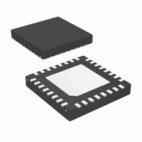
LMH1982SQE/NOPB National Semiconductor, LMH1982SQE/NOPB Datasheet - Page 27

LMH1982SQE/NOPB
Manufacturer Part Number
LMH1982SQE/NOPB
Description
IC CLK GEN MULTI RATE VID 32-LLP
Manufacturer
National Semiconductor
Type
Clock Generatorr
Datasheet
1.LMH1982SQENOPB.pdf
(34 pages)
Specifications of LMH1982SQE/NOPB
Applications
Displays, Projectors, Receivers
Mounting Type
Surface Mount
Package / Case
32-LLP
For Use With
LMH1982SQEEVAL - BOARD EVAL FOR LMH1982SQE
Lead Free Status / RoHS Status
Lead free / RoHS Compliant
Other names
LMH1982SQETR
Bit 5: Pin 6 Override (PIN6_OVRD)
The PIN6_OVRD bit can be programmed to override the de-
fault reference selection capability on pin 6 and instead use
pin 6 as an logic pulse input to initialize or reset the internal
counters for output initialization.
pin 6 for reference selection if RSEL_I
RSEL_I
is controlled via I
via I
ister 0Ah).
pin 6 for output initialization if EN_TOF_RST = 1. If
EN_TOF_RST = 0, then any TOF Init pulse received at pin 6
will be ignored. Additionally, reference selection must be con-
trolled via I
Bits 7-6: Reserved (RSV)
These RSV bits are reserved. When writing to this register,
only write the default data to the RSV bits as specified in Table
8.
9.4 PLL 1 Divider Register
Register 03h
Bits 1-0: Reference Divider Selection (REF_DIV_SEL)
REF_DIV_SEL selects the reference divider value according
to the selection table in Table 2. See section 4.1 Programming
the PLL 1 Dividers.
The reference divider value is the denominator of PLL 1's di-
vider ratio:
Feedback divider value / Reference divider value = 27 MHz /
Hsync input frequency
The numerator and denominator values of the divider ratio
should be reduced to their lowest factors to be compatible with
the range of divider values offered by REF_DIV_SEL and
FB_DIV. These registers must be programmed correctly to
phase lock the 27 MHz VCXO PLL and output clocks to the
input reference. See Table 1 for the suggested divider set-
tings for the supported timing formats.
Bits 7-3: Reserved (RSV)
These RSV bits are reserved. When writing to this register,
only write the default data to the RSV bits as specified in Table
8.
Register 04h
Bits 7-0: Feedback Divider (FB_DIV)
This register contains the 8 LSBs of FB_DIV. The feedback
divider value is the numerator of PLL 1's divider ratio. FB_DIV
should be programmed using the feedback divider value after
the divide ratio has been reduced to its lowest factors. Refer
to the description for register 03h, and see Table 1 for the
suggested divider settings for the supported timing format.
Register 05h
Bits 4-0: Feedback Divider (FB_DIV)
This register contains the 5 MSBs of FB_DIV. See the de-
scription for register 04h.
Bits 7-5: These non-programmable bits contain zeros.
PIN6_OVRD = 0: Allows a logic level input to be applied to
PIN6_OVRD = 1: Allows an TOF Init pulse to be applied to
2
C by programming TOF_INIT and EN_TOF_RST (reg-
filter design will be necessarily different between the 27 MHz input
and H sync inputs. Alternatively, it's possible to use an external
counter circuit to divide the 27 MHz clock to a lower frequency (e.g.
like H sync) input, so only one loop filter design could support both
types of inputs.
2
C = 1, then pin 6 is ignored and reference selection
2
C, regardless of I
2
C; additionally, outputs must be initialized
2
C_RSEL.
2
C = 0 (register 00h). If
27
9.5 PLL 4 Charge Pump Current Control Register
Register 06h
Bits 3-0: Charge Pump Current Control for PLL 4 (ICP4)
ICP4 can be programmed to specify charge pump current for
PLL 4, which generates the 67.5 MHz SD clock.
Note: Bit 3 is inverted internally, so the default ICP4 value of 0000b (0h)
The PLL 4 charge pump current increases linearly with the
effective value. Reducing the effective value of the charge
pump current will lower its loop bandwidth at the expense of
reduced PLL stability. An effective value of 0 (ICP4 = 1000b)
should not be programmed since this corresponds to 0 µA
nominal current and will cause PLL 4 to lose phase lock.
Bits 7-4: Reserved (RSV)
These RSV bits are reserved. When writing to this register,
only write the default data to the RSV bits as specified in Table
8.
Register 07h
Bits 7-0: Reserved (RSV)
This register is reserved. If necessary, only write the default
data (00h) to register 07h as specified in Table 8.
9.6 Output Clock And TOF Control Register
Register 08h
Bit 0: SD Clock Output Frequency Select (SD_FREQ)
This bit sets the clock frequency of the SD_CLK output pair.
Bit 1: SD Clock Output Mode (SD_HIZ)
Set the SD_HIZ bit to 1 to put the SD_CLK output pair in high-
impedance (Hi-Z) mode; otherwise, the SD_CLK output will
be enabled.
Bit 3-2: HD Clock Output Frequency Select (HD_FREQ)
These bits set the clock frequency of the HD_CLK output pair.
Note: When selecting the 148.35 MHz clock, you must also program the
Bit 4: HD Clock Output Mode (HD_HIZ)
Set the HD_HIZ bit to 1 to put the HD_CLK output pair in high-
impedance (Hi-Z) mode; otherwise, the HD_CLK output will
be enabled.
Bit 5: Top of Frame Output Mode (TOF_HIZ)
Set the TOF_HIZ bit to 1 to put the TOF output pin in high-
impedance (Hi-Z) mode; otherwise, the output will be en-
abled.
Bits 7-6: Reserved (RSV)
These RSV bits are reserved. When writing to this register,
only write the default data to the RSV bits as specified in Table
8.
9.7 TOF Configuration Registers
Register 09h
SD_FREQ = 0: Selects 27 MHz from PLL 1.
SD_FREQ = 1: Selects 67.5 MHz from PLL 4.
HD_FREQ = 0h: Selects 74.25 MHz from PLL 2.
HD_FREQ = 1h: Selects 74.176 MHz from PLL 3.
HD_FREQ = 2h: Selects 148.5 MHz from PLL 2.
HD_FREQ = 3h: Selects 148.35 MHz from PLL 3.
actually yields an effective value of 1000b (8h), which is the mid-scale
setting.
PLL 3 initialization sequence as described in section 2.1 148.35 MHz
PLL Initialization Sequence.
www.national.com


